 ChipApex | Global Electronic Components Supplier
SEARCH
Search Product
Search Post
— IC芯片 | 连接器 | 传感器 | 被动器件 —
Search productSearch post
— IC芯片 | 连接器 | 传感器 | 被动器件 —
Consult the customer manager about the wholesale price.
consultation hotline:86-132-6715-2157
email:[email protected]
Contact the product manager for consultation. One-stop consultation is available.
Do you want a lower wholesale price? Please send us your inquiry and we will reply immediately.
The TC7QPB9307FK(EL) is a CMOS 4-bit dual-supply bus switch designed for bidirectional level-shifting between nodes operating at different voltage levels. It supports VCCA ranges of 1.65 V to 5.0 V and VCCB ranges of 2.3 V to 5.5 V. The device features an active-Low Output Enable (OE) input that controls all four channels simultaneously. Key electrical parameters include a maximum ON-resistance of 8.0 Ω, propagation delay times ranging from 0.3 ns to 2.2 ns depending on supply conditions, and quiescent supply currents up to 4.0 µA. It operates within a temperature range of -40°C to +85°C.
Verify the specific ordering suffix matches the required package configuration, as the base part number TC7QPB9307FK corresponds to the VSSOP14 (US14) package. Confirm RoHS compliance status through official Toshiba documentation or authorized distributors prior to procurement. Ensure design reviews account for the absolute maximum ratings to prevent device deterioration.
Select this component when a 4-bit bidirectional bus switch with an active-Low enable signal is required. It is suitable for applications needing simultaneous switching of multiple data lines across different voltage domains. Consider the 8.0 Ω maximum ON-resistance and low leakage characteristics for signal integrity in low-power designs requiring robust power-down protection.
This device belongs to the TC7QPB series of low-voltage, low-power CMOS digital integrated circuits manufactured by Toshiba Semiconductor and Storage. It is functionally paired with the TC7QPB9306FK, which differs only in having an active-High Output Enable input. Both parts share identical electrical specifications and packaging options.
The TC7QPB9306FK serves as a direct functional substitute if an active-High Output Enable signal is preferred instead of the active-Low configuration found in the TC7QPB9307FK. Other members of the TC7MPB or TC7WPB series may offer similar bus switching capabilities but require verification of pinout compatibility and specific electrical parameter alignment.
The OE input is active-Low. When OE is Low, the switch connects the A port to the B port. When OE is High, the switch disconnects the ports, effectively isolating the buses.
VCCA supports a range of 1.65 V to 5.0 V, while VCCB supports a range of 2.3 V to 5.5 V. The VCCA voltage must be lower than the VCCB voltage for normal operation.
Yes, the device supports power-down protection at the OE input, which is rated for 5.5 V tolerance, ensuring safe operation even when one of the power supplies is off.
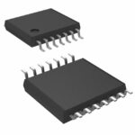 TC7QPB9307FK(EL)
The activity of extra discounts on wholesale prices is in full swing…
Please fill in your contact information and we will send you the latest wholesale price list.






