 ChipApex | Global Electronic Components Supplier
SEARCH
Search Product
Search Post
— IC芯片 | 连接器 | 传感器 | 被动器件 —
Search productSearch post
— IC芯片 | 连接器 | 传感器 | 被动器件 —
Consult the customer manager about the wholesale price.
consultation hotline:86-132-6715-2157
email:[email protected]
Contact the product manager for consultation. One-stop consultation is available.
Do you want a lower wholesale price? Please send us your inquiry and we will reply immediately.
The TC7SET126F,LJ(CT is a single-channel, non-inverting bus buffer with three-state outputs manufactured by Toshiba Semiconductor and Storage. It operates within a supply voltage range of 4.5 V to 5.5 V and utilizes L-MOS logic technology. The device features TTL-compatible input thresholds (VIL max 0.8 V, VIH min 2.0 V) and 5.5 V tolerant inputs. It supports an operating temperature range of -40 °C to 85 °C for this specific suffix. Key electrical parameters include a maximum quiescent current of 20 µA at -40 to 85 °C, high-level output current of -8 mA, and low-level output current of 8 mA. Propagation delay is typically 3.7 ns at 5.0 V.
Verify the ordering suffix J(CT) confirms the -40 °C to 85 °C operating temperature range, as other suffixes may support up to 125 °C. Confirm RoHS compliance status directly with the manufacturer or authorized distributors, as environmental declarations are subject to change. Ensure the SMV package type matches the PCB footprint requirements. Cross-reference the latest datasheet revision to verify any updates to absolute maximum ratings or electrical characteristics before finalizing procurement specifications.
Select this component when a single-channel, non-inverting buffer with three-state control is required for 5 V logic systems. It is suitable for designs needing TTL compatibility and 5.5 V input tolerance. Consider the SMV surface-mount package for space-constrained layouts. Verify that the required operating temperature range aligns with the -40 °C to 85 °C specification associated with the LJ(CT) suffix. Ensure the application does not exceed the absolute maximum ratings for supply voltage or output current.
The TC7SET126F belongs to Toshiba's TC7SET series of CMOS digital integrated circuits. This series focuses on high-speed, low-power performance using L-MOS technology. The device functions as a bus buffer, facilitating data transfer between different parts of a digital system while providing isolation through its three-state output capability. It is part of a broader family of logic ICs designed for various digital switching and buffering applications.
Publicly confirmed substitute part numbers are not available in the provided source material. Consult Toshiba sales representatives for alternative recommendations if this specific part number is unavailable.
For devices with the ordering part number ending in J(CT), the operating temperature range is -40 °C to 85 °C.
Yes, the device is compatible with TTL outputs, with a maximum low-level input voltage (VIL) of 0.8 V and a minimum high-level input voltage (VIH) of 2.0 V.
Yes, the device is compliant with the reliability requirements of AEC-Q100.
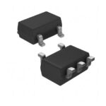 TC7SET126F,LJ(CT
The activity of extra discounts on wholesale prices is in full swing…
Please fill in your contact information and we will send you the latest wholesale price list.




