 ChipApex | Global Electronic Components Supplier
SEARCH
Search Product
Search Post
— IC芯片 | 连接器 | 传感器 | 被动器件 —
Search productSearch post
— IC芯片 | 连接器 | 传感器 | 被动器件 —
Consult the customer manager about the wholesale price.
consultation hotline:86-132-6715-2157
email:[email protected]
Contact the product manager for consultation. One-stop consultation is available.
Do you want a lower wholesale price? Please send us your inquiry and we will reply immediately.
The TC7SH125FU,LJ(CT is a single-channel bus buffer with 3-state output from Toshiba's L-MOS family. It operates within a supply voltage range of 2.0 to 5.5 V and features 5.5 V tolerant inputs. The device supports an operating temperature range of -40 to 85 °C for this specific suffix. Key electrical characteristics include a maximum quiescent supply current of 20 µA at extended temperatures, high noise immunity defined as 28% of VCC minimum, and propagation delays typically ranging from 3.8 ns to 11.0 ns depending on load and voltage conditions.
Verify the ordering suffix J(CT) confirms the -40 to 85 °C operating temperature range, distinct from the standard -40 to 125 °C rating. Confirm RoHS compliance status directly with the manufacturer or authorized distributors as environmental declarations may vary by production batch. Ensure packaging specifications match system assembly requirements.
Select this component when a single-channel non-inverting buffer with controlled 3-state outputs is required. The wide supply voltage range accommodates various logic families. Consider the package size and pinout compatibility during PCB layout. Verify that the input capacitance and drive strength meet the specific bus loading requirements of the target application circuit.
This part belongs to Toshiba's L-MOS (Low Voltage MOS) series, designed for low-power digital applications. The SH series specifically denotes high-speed operation within the CMOS logic portfolio. The USV package corresponds to the SOT-353 form factor, providing a compact solution for space-constrained designs requiring reliable signal buffering.
Check for direct substitutes within the TC7SH125 family with different suffixes if wider temperature ranges are acceptable. Cross-reference with other single-buffer 3-state logic ICs ensuring identical pinouts and voltage tolerances to avoid redesign efforts.
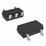 TC7SH125FU,LJ(CT
The activity of extra discounts on wholesale prices is in full swing…
Please fill in your contact information and we will send you the latest wholesale price list.





