 ChipApex | Global Electronic Components Supplier
SEARCH
Search Product
Search Post
— IC芯片 | 连接器 | 传感器 | 被动器件 —
Search productSearch post
— IC芯片 | 连接器 | 传感器 | 被动器件 —
Consult the customer manager about the wholesale price.
consultation hotline:86-132-6715-2157
email:[email protected]
Contact the product manager for consultation. One-stop consultation is available.
Do you want a lower wholesale price? Please send us your inquiry and we will reply immediately.
The TC7SH126FU,LJ(CT is a single-channel, non-inverting bus buffer with 3-state output manufactured by Toshiba Semiconductor and Storage. It operates within a supply voltage range of 2.0 V to 5.5 V and features 5.5 V tolerant inputs. The device supports a wide operating temperature range of -40°C to 85°C for the J(CT suffix variant. Key electrical characteristics include a maximum quiescent current of 2.0 µA at 25°C and high noise immunity defined as 28% of VCC minimum. Propagation delay is typically 3.8 ns at 5.0 V with a 15 pF load.
Verify that the specific ordering suffix matches the required temperature grade, as the J(CT suffix restricts the operating range to -40°C to 85°C compared to other variants. Confirm package compatibility with the USV (SOT-353) footprint during PCB layout. Ensure input pins are tied to VCC or GND when unused to maintain stable operation and prevent undefined states.
Select this component for applications requiring a single-channel buffer with 3-state control and 5.5 V input tolerance. Consider the specific temperature rating associated with the ordering suffix when designing for automotive or industrial environments. Evaluate the power dissipation capacitance and quiescent current requirements against system power budgets to ensure compliance with low-power design constraints.
This part belongs to the TC7SH series of CMOS digital integrated circuits from Toshiba. It functions as a silicon monolithic device designed for general-purpose logic applications. The series emphasizes low power consumption and high speed, making it suitable for portable and battery-operated electronic equipment where efficient power management is critical.
Check for alternative parts within the same TC7SH family or compatible L-MOS logic families. Verify pinout compatibility and electrical parameter alignment, particularly regarding 3-state enable timing and input voltage tolerances, before substituting.
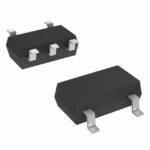 TC7SH126FU,LJ(CT
The activity of extra discounts on wholesale prices is in full swing…
Please fill in your contact information and we will send you the latest wholesale price list.





