 ChipApex | Global Electronic Components Supplier
SEARCH
Search Product
Search Post
— IC芯片 | 连接器 | 传感器 | 被动器件 —
Search productSearch post
— IC芯片 | 连接器 | 传感器 | 被动器件 —
Consult the customer manager about the wholesale price.
consultation hotline:86-132-6715-2157
email:[email protected]
Contact the product manager for consultation. One-stop consultation is available.
Do you want a lower wholesale price? Please send us your inquiry and we will reply immediately.
The TC7SPB9307TU,LF is a CMOS 1-bit dual-supply bus switch designed for bidirectional level-shifting between nodes operating at different voltage levels. It features an active-Low Output Enable (OE) control signal and supports independent power supplies VCCA (1.65V to 5.0V) and VCCB (2.3V to 5.5V). The device provides 5.5V tolerance and power-down protection at the OE input. It utilizes n-type MOSFET channels with a typical ON-resistance of 5.0Ω and operates within a temperature range of -40°C to 85°C in a UF6 package.
Verify the specific ordering suffix corresponds to the LF designation for lead-free compliance. Confirm the UF6 package type matches the target footprint requirements. Ensure the design accounts for the active-Low OE functionality distinct from the TC7SPB9306TU variant. Validate that the application voltage ranges fall within the specified VCCA and VCCB operational limits defined in the datasheet.
Select this component when a single-channel bidirectional switch with active-Low enable control is required. It is suitable for interfacing low-voltage logic with higher-voltage domains up to 5.5V. Consider the UF6 package constraints for board space. Compare against the TC7SPB9306TU if an active-High enable signal is preferred instead.
This part belongs to the TC7SPB series of low-voltage, low-power CMOS digital integrated circuits manufactured by Toshiba Semiconductor and Storage. It is functionally paired with the TC7SPB9306TU, differing primarily in the polarity of the Output Enable control signal. Both devices share similar electrical characteristics and packaging options for dual-supply bus switching applications.
The TC7SPB9306TU serves as a functional alternative but requires inversion of the enable signal logic due to its active-High OE configuration. No other direct substitutes are confirmed in the provided documentation.
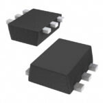 TC7SPB9307TU,LF
The activity of extra discounts on wholesale prices is in full swing…
Please fill in your contact information and we will send you the latest wholesale price list.





