 ChipApex | Global Electronic Components Supplier
SEARCH
Search Product
Search Post
— IC芯片 | 连接器 | 传感器 | 被动器件 —
Search productSearch post
— IC芯片 | 连接器 | 传感器 | 被动器件 —
Consult the customer manager about the wholesale price.
consultation hotline:86-132-6715-2157
email:[email protected]
Contact the product manager for consultation. One-stop consultation is available.
Do you want a lower wholesale price? Please send us your inquiry and we will reply immediately.
The TC7SZ34F(T5L,JF,T) is a single-channel non-inverter buffer manufactured by Toshiba Semiconductor and Storage. It operates within a supply voltage range of 1.65 V to 5.5 V and features 5.5 V tolerant inputs with power-down protection outputs. The device supports an operating temperature range of -40 °C to 125 °C, excluding suffixes ending in J(CT). Key electrical specifications include a typical propagation delay of 2.4 ns at 5.0 V with 50 pF load, minimum output current of ±24 mA at 3.0 V, and input capacitance of 4 pF.
Verify the specific ordering suffix to confirm the operating temperature range. Devices with suffixes ending in J(CT) are rated for -40 °C to 85 °C, while other variants support -40 °C to 125 °C. Ensure compatibility with required packaging formats such as SMV (SOT-753). Confirm RoHS compliance status with the manufacturer prior to procurement.
Select this component when a single-channel non-inverting buffer with high drive strength is required. It is suitable for applications needing 5.5 V tolerance on inputs while operating at lower supply voltages down to 1.65 V. Consider the extended temperature range (-40 °C to 125 °C) for harsh environments, noting that specific suffixes may limit this range. Compare propagation delays against system timing requirements under specific load conditions.
This part belongs to the TC7SZ series of CMOS digital integrated circuits from Toshiba. It is designed as a small-scale logic buffer offering high speed and low power consumption. The series is characterized by its ability to operate across a wide voltage range and its compatibility with various logic standards, making it versatile for modern digital designs.
The datasheet notes performance matching with the TC74LCX series when operated at 3.3 V. Verify pinout and electrical characteristics before substituting with other single-buffer ICs.
Standard versions support an operating temperature range of -40 °C to 125 °C. Devices with ordering part numbers ending in J(CT) are restricted to a range of -40 °C to 85 °C.
Yes, the device includes 5.5 V power-down protection outputs, allowing it to withstand voltage levels up to 5.5 V even when the supply voltage is zero.
The typical propagation delay (tpd) is 2.4 ns when measured at a supply voltage of 5.0 V with a capacitive load of 50 pF.
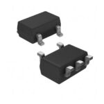 TC7SZ34F(T5L,JF,T)
The activity of extra discounts on wholesale prices is in full swing…
Please fill in your contact information and we will send you the latest wholesale price list.





