 ChipApex | Global Electronic Components Supplier
SEARCH
Search Product
Search Post
— IC芯片 | 连接器 | 传感器 | 被动器件 —
Search productSearch post
— IC芯片 | 连接器 | 传感器 | 被动器件 —
Consult the customer manager about the wholesale price.
consultation hotline:86-132-6715-2157
email:[email protected]
Contact the product manager for consultation. One-stop consultation is available.
Do you want a lower wholesale price? Please send us your inquiry and we will reply immediately.
The TC7W126FUTE12LF is a dual bus buffer utilizing C2MOS technology, providing non-inverting logic with three-state outputs. It operates within a supply voltage range of 2 V to 6 V and supports an operating temperature from -40°C to +85°C. The device features a typical propagation delay of 10 ns at 5 V and maintains a maximum quiescent current of 2 µA. Output drive capability supports up to 15 LSTTL loads, with symmetrical output impedance ensuring balanced signal transitions.
Verify the specific ordering suffix matches the required package configuration before procurement. Confirm RoHS compliance status directly with the manufacturer or authorized distributor as environmental declarations may vary by production lot. Ensure the component meets the intended application's reliability requirements by consulting the Toshiba Semiconductor Reliability Handbook.
Select this component for designs requiring wide voltage compatibility between 2 V and 6 V. The C2MOS process offers a balance of speed and power efficiency suitable for battery-operated devices. Verify that the SSOP-8 package dimensions align with the PCB footprint constraints and that the thermal dissipation capabilities are sufficient for the expected operating environment.
This part belongs to the TC7W126 series of dual bus buffers manufactured by Toshiba Semiconductor and Storage. The 'FU' designation indicates the standard SSOP-8 package, while the 'TE12LF' suffix specifies the tape and reel packaging format with lead-free composition. This series is designed for general-purpose digital logic buffering in compact electronic assemblies.
TC7W125FUTE12LF (Non-inverting variant)
The G input serves as the three-state control. Setting it low places the outputs into a high-impedance state, effectively disconnecting them from the bus.
The device provides high noise immunity with minimum noise input voltages (VNIH and VNIL) defined as 28% of the supply voltage (VCC).
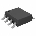 TC7W126FUTE12LF
The activity of extra discounts on wholesale prices is in full swing…
Please fill in your contact information and we will send you the latest wholesale price list.





