 ChipApex | Global Electronic Components Supplier
SEARCH
Search Product
Search Post
— IC芯片 | 连接器 | 传感器 | 被动器件 —
Search productSearch post
— IC芯片 | 连接器 | 传感器 | 被动器件 —
Consult the customer manager about the wholesale price.
consultation hotline:86-132-6715-2157
email:[email protected]
Contact the product manager for consultation. One-stop consultation is available.
Do you want a lower wholesale price? Please send us your inquiry and we will reply immediately.
The TC7W66FK,LF is a dual bilateral switch IC from Toshiba Semiconductor and Storage, housed in an US8 package. It operates on a supply voltage (VCC) ranging from 2 V to 12 V and supports an operating temperature range of -40 °C to +85 °C. The device features a typical propagation delay (tpd) of 7 ns at 5 V, with a maximum quiescent supply current (ICC) of 1 μA at 25 °C. Typical ON resistance (RON) is 50 Ω at 9 V, and total harmonic distortion (THD) is 0.05% at 5 V.
Verify the specific ordering suffix matches the required package type, as the FK suffix denotes the US8 package configuration. Confirm RoHS compliance status through official Toshiba documentation before procurement. Ensure the component meets the intended environmental operating temperature requirements during selection.
Select this component when a dual bilateral switch is required for both digital and analog signal paths within a single package. Consider the 2 V to 12 V supply range and the specific ON resistance characteristics relative to the load current. Verify that the US8 package dimensions align with the PCB layout constraints.
This part belongs to the TC7W series of CMOS digital integrated circuits manufactured by Toshiba Semiconductor and Storage. It serves as a high-speed bilateral switch designed for applications requiring low power consumption and high linearity. The device is functionally compatible with other similar bilateral switches in the industry.
The datasheet indicates pin and function compatibility with the TC4W66. Verify electrical specifications and package dimensions match the original design requirements before substitution.
The TC7W66FU uses an SM8 package, while the TC7W66FK utilizes a US8 package. Both contain the same internal circuitry but differ in physical footprint and weight.
The switch turns ON when the control input (C) is high and turns OFF when the control input is low.
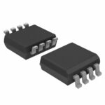 TC7W66FK,LF
The activity of extra discounts on wholesale prices is in full swing…
Please fill in your contact information and we will send you the latest wholesale price list.





