 ChipApex | Global Electronic Components Supplier
SEARCH
Search Product
Search Post
— IC芯片 | 连接器 | 传感器 | 被动器件 —
Search productSearch post
— IC芯片 | 连接器 | 传感器 | 被动器件 —
Consult the customer manager about the wholesale price.
consultation hotline:86-132-6715-2157
email:[email protected]
Contact the product manager for consultation. One-stop consultation is available.
Do you want a lower wholesale price? Please send us your inquiry and we will reply immediately.
The TC7WB126FK is a dual bus switch manufactured by Toshiba Semiconductor and Storage. It operates within a supply voltage range of 4.5 to 5.5 V. The device features an ultra-low on-resistance with a typical value of 5 Ω. Propagation delay is specified at a maximum of 0.25 ns. Quiescent supply current is limited to 10 μA. Input leakage current does not exceed ±1.0 μA. Power dissipation is rated at 200 mW. The component utilizes the US8 package.
Verify that the operating environment remains within the specified temperature range of -40 to 85 °C. Ensure the supply voltage stays between 4.5 and 5.5 V to maintain proper functionality. Unused inputs must be connected to either VCC or GND to prevent undefined states. Confirm compliance with RoHS directives if required by your specific application standards.
Select this component when low on-resistance and fast switching speeds are critical requirements. It is suitable for designs requiring operation strictly within the 4.5 to 5.5 V supply range. Consider its small form factor and low power profile for space-constrained or battery-operated devices. Verify that the input voltage levels align with the TTL level input specifications provided.
This part belongs to the TC7WB series of CMOS digital integrated circuits. It functions as a dual-bit bus switch designed for connecting or disconnecting ports with minimal delay. The device is built using silicon monolithic technology, ensuring reliability and consistent performance across various industrial and commercial electronic applications.
PUMH16,115 is listed as a similar alternative part number from Nexperia USA Inc.
The maximum propagation delay time (tpLH/tpHL) is 0.25 ns when measured under standard test conditions.
When the Output Enable (OE) pin is at a High level, the switch connects the A port to the B port. When OE is Low, the switch disconnects the ports.
The typical on-resistance (RON) is 5 Ω, measured at a supply voltage of 5 V and room temperature.
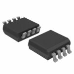 TC7WB126FK(TE85L,F
The activity of extra discounts on wholesale prices is in full swing…
Please fill in your contact information and we will send you the latest wholesale price list.





