 ChipApex | Global Electronic Components Supplier
SEARCH
Search Product
Search Post
— IC芯片 | 连接器 | 传感器 | 被动器件 —
Search productSearch post
— IC芯片 | 连接器 | 传感器 | 被动器件 —
Consult the customer manager about the wholesale price.
consultation hotline:86-132-6715-2157
email:[email protected]
Contact the product manager for consultation. One-stop consultation is available.
Do you want a lower wholesale price? Please send us your inquiry and we will reply immediately.
The TC7WB66CL8X,LF is a dual SPST bus switch manufactured by Toshiba Semiconductor and Storage. It operates within a supply voltage range of 1.65 V to 5.5 V and supports an operating temperature range of -40 °C to 125 °C. The device features low on-resistance with typical values between 4 Ω and 9 Ω depending on voltage and current conditions. Input capacitance is typically 4 pF, while switch terminal capacitance is 5 pF when active and 10 pF when inactive. Propagation delays are specified up to 18 ns at 5.0 V. The component utilizes a US8 package.
Verify the specific ordering suffix to confirm the operating temperature range, as devices ending in (CT) differ from standard versions. Confirm AEC-Q100 compliance details directly with Toshiba sales representatives if automotive qualification is required. Ensure design adheres to the provided derating concepts and handling precautions outlined in the Toshiba Semiconductor Reliability Handbook.
Select this component for applications requiring bidirectional data transfer with minimal propagation delay. The wide supply voltage range allows compatibility with various logic families. Consider the ON-resistance characteristics relative to the expected load current to ensure signal integrity. Verify that the US8 package dimensions fit the target PCB layout constraints.
This part belongs to the TC7WB66CFK/TC7WB67CFK series of CMOS digital integrated circuits. It functions as a silicon monolithic device designed for efficient bus switching. The series emphasizes low power consumption inherent to CMOS technology while maintaining high-speed performance capabilities suitable for modern digital interfaces.
Public confirmed substitute part numbers are not available in the source material.
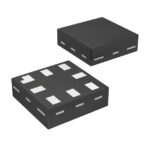 TC7WB66CL8X,LF
The activity of extra discounts on wholesale prices is in full swing…
Please fill in your contact information and we will send you the latest wholesale price list.






