 ChipApex | Global Electronic Components Supplier
SEARCH
Search Product
Search Post
— IC芯片 | 连接器 | 传感器 | 被动器件 —
Search productSearch post
— IC芯片 | 连接器 | 传感器 | 被动器件 —
Consult the customer manager about the wholesale price.
consultation hotline:86-132-6715-2157
email:[email protected]
Contact the product manager for consultation. One-stop consultation is available.
Do you want a lower wholesale price? Please send us your inquiry and we will reply immediately.
The TC7WBL3306CFK,L(CT is a low-voltage, low-capacitance CMOS dual bus switch manufactured by Toshiba Semiconductor and Storage. It operates within a supply voltage range of 1.65 V to 3.6 V and features an ON-resistance of 6.0 Ω typical at 3.0 V with zero input signal voltage. The device includes power-down protection for inputs and outputs, ensuring minimal leakage current during standby modes. It utilizes an 8-pin US8 package and supports an operating temperature range from -40°C to 85°C.
Verify the specific suffix L(CT corresponds to the required packaging format, such as cut tape or reel, before finalizing orders. Confirm RoHS compliance status through official manufacturer documentation to ensure adherence to environmental regulations. Cross-reference the part number with authorized distributors to validate authenticity and traceability.
Select this component for applications demanding low propagation delay and minimal signal attenuation. Ensure the control logic aligns with the active-high output enable requirement specific to the 3306 variant. Evaluate the maximum allowable ON-resistance against the target circuit's voltage drop constraints to maintain signal integrity across the operational temperature range.
This device belongs to the TC7WBL series of low-voltage bus switches designed for portable applications. It shares architectural similarities with the TC7WBL3305 but differs in control polarity. The series addresses the need for efficient signal management in battery-operated devices where power conservation and signal fidelity are critical design parameters.
Direct substitutes include the TC7WBL3305CFK,LF, which offers identical electrical characteristics but utilizes an active-low output enable configuration. Verify pin compatibility and control logic inversion requirements when transitioning between these variants to prevent functional mismatches in existing designs.
The TC7WBL3306 requires the OE input to be set high to activate the switch, whereas the TC7WBL3305 requires the OE input to be set low for activation.
The typical ON-capacitance (CI/O) is 7 pF when measured at a supply voltage of 3.0 V.
Yes, the inputs and I/O pins are equipped with power-down protection circuits to limit leakage current when the supply voltage is absent.
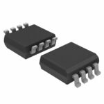 TC7WBL3306CFK,L(CT
The activity of extra discounts on wholesale prices is in full swing…
Please fill in your contact information and we will send you the latest wholesale price list.





