 ChipApex | Global Electronic Components Supplier
SEARCH
Search Product
Search Post
— IC芯片 | 连接器 | 传感器 | 被动器件 —
Search productSearch post
— IC芯片 | 连接器 | 传感器 | 被动器件 —
Consult the customer manager about the wholesale price.
consultation hotline:86-132-6715-2157
email:[email protected]
Contact the product manager for consultation. One-stop consultation is available.
Do you want a lower wholesale price? Please send us your inquiry and we will reply immediately.
The TC7WH241FUTE12LF is a Toshiba CMOS digital integrated circuit functioning as a dual bus buffer with non-inverted, 3-state outputs. It operates within a supply voltage range of 2.0 V to 5.5 V and supports an operating temperature from -40°C to +85°C. The device features high-speed performance with typical propagation delays of 3.6 ns at 5 V and low power dissipation with a maximum quiescent current of 2 μA. It includes 5.5-V tolerant inputs and balanced propagation delays.
Verify that the specific ordering suffix matches the required package type and tape-and-reel specifications. Confirm RoHS compliance status directly with the manufacturer or authorized distributor documentation before finalizing procurement orders.
Select this component when designing systems requiring dual-channel buffering with controlled impedance and 3-state isolation. Ensure the application voltage remains within the 2.0 V to 5.5 V range and consider the SSOP-8 package constraints for PCB layout.
This part belongs to the TC7WH series of Toshiba CMOS logic ICs. It shares functional similarities with other buffers in the family but is distinguished by its specific dual-channel architecture and non-inverting signal path characteristics defined in the official datasheet.
Consult official Toshiba cross-reference lists for verified substitutes. Do not assume pin-compatible alternatives without verifying electrical parameters and package dimensions against the original specification sheet.
The G input acts as the control signal; when High, the outputs enter a high-impedance state, effectively disconnecting them from the bus.
The inputs are designed to be 5.5-V tolerant, allowing safe operation even if input signals exceed the local supply voltage up to that limit.
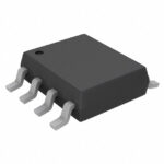 TC7WH241FUTE12LF
The activity of extra discounts on wholesale prices is in full swing…
Please fill in your contact information and we will send you the latest wholesale price list.





