 ChipApex | Global Electronic Components Supplier
SEARCH
Search Product
Search Post
— IC芯片 | 连接器 | 传感器 | 被动器件 —
Search productSearch post
— IC芯片 | 连接器 | 传感器 | 被动器件 —
Consult the customer manager about the wholesale price.
consultation hotline:86-132-6715-2157
email:[email protected]
Contact the product manager for consultation. One-stop consultation is available.
Do you want a lower wholesale price? Please send us your inquiry and we will reply immediately.
The TC7WP3125FK is a dual-supply, advanced high-speed CMOS 2-bit bus buffer fabricated with silicon gate technology. It facilitates interface between low-voltage buses (1.2 V to 2.5 V) and higher voltage buses (1.8 V to 3.6 V). The device features overvoltage tolerant inputs and outputs up to 3.6 V. Operating supply ranges include VCCA from 1.1 V to 2.7 V and VCCB from 1.65 V to 3.6 V. Propagation delay varies by voltage configuration, ranging from 6.8 ns at VCCA=2.5V/VCCB=3.3V to 30 ns at VCCA=1.2V/VCCB=1.8V. Output drive capability reaches 12 mA minimum at VCCB=3.0V.
Verify the specific ordering suffix to confirm the operating temperature range. Devices ending in (CT) are rated for -40°C to 85°C, while other suffixes support -40°C to 125°C. Confirm package availability matches the US8 form factor. Ensure design accounts for absolute maximum ratings regarding supply voltage differentials between VCCA and VCCB pins.
Select this component when bridging disparate voltage domains within a single system. It supports multiple VCCA/VCCB combinations including 1.2V/3.3V, 1.5V/2.5V, and 1.8V/3.6V. Consider the propagation delay specifications relative to the target bus speed. The US8 package is suitable for space-constrained designs. Verify that the required output current aligns with the load capacitance and drive requirements.
This part belongs to Toshiba's TC7WP series of low-voltage, low-power CMOS digital integrated circuits. It utilizes silicon gate CMOS technology for high-speed operation. The device is designed specifically for data bus applications requiring voltage translation between different logic families or supply rails.
TC7WPN3125FK(T5L,F)
Yes, the A-bus is permitted to float when the OE input is High.
Applying a signal to any bus pins while in the output mode may result in damage to the device.
No, VCCB should not be supplied with voltage when VCCA is in the OFF state.
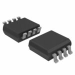 TC7WP3125FK(T5L,F)
The activity of extra discounts on wholesale prices is in full swing…
Please fill in your contact information and we will send you the latest wholesale price list.





