 ChipApex | Global Electronic Components Supplier
SEARCH
Search Product
Search Post
— IC芯片 | 连接器 | 传感器 | 被动器件 —
Search productSearch post
— IC芯片 | 连接器 | 传感器 | 被动器件 —
Consult the customer manager about the wholesale price.
consultation hotline:86-132-6715-2157
email:[email protected]
Contact the product manager for consultation. One-stop consultation is available.
Do you want a lower wholesale price? Please send us your inquiry and we will reply immediately.
The TC7WPN3125FK,LF(CT is a dual-supply, advanced high-speed CMOS 2-bit bus buffer designed for mixed-voltage systems. It interfaces between A-bus (VCCA: 1.1 V to 2.7 V) and B-bus (VCCB: 1.65 V to 3.6 V). The device supports operating temperatures of -40°C to 85°C. Key electrical parameters include propagation delays ranging from 13.7 ns to 43 ns depending on supply voltages, and output currents of up to 3 mA minimum at VCCB = 3.0 V. Inputs and outputs tolerate up to 3.6 V with power-down protection.
Verify the ordering suffix (CT) confirms the -40°C to 85°C operating temperature range, distinct from other variants. Confirm RoHS compliance status directly with Toshiba Semiconductor and Storage. Ensure design adheres to absolute maximum ratings, specifically avoiding voltage application to VCCB while VCCA is off. Review the Toshiba Semiconductor Reliability Handbook for derating guidelines.
Select this component for bidirectional data transfer between disparate voltage domains within the specified ranges. The US8 package suits space-constrained designs. Consider the propagation delay variations relative to specific VCCA and VCCB combinations. Ensure unused inputs are tied to VCC or GND to maintain stable operation. Validate that the required output current capabilities meet the load requirements of the destination bus.
This part belongs to the TC7WP series of low-voltage, low-power CMOS digital integrated circuits. It utilizes silicon gate CMOS technology for high-speed operation. The device functions as a bus buffer rather than a simple switch, facilitating level shifting between two independent power supplies. It is manufactured by Toshiba Electronic Devices & Storage Corporation.
Toshiba recommends the TC7WP3125FK,LF(CT as a manufacturer-recommended substitute. Verify pinout compatibility and electrical specifications before substitution.
All inputs and outputs are tolerant up to 3.6 V and include power-down protection.
When OE is High, the device disables, effectively isolating the signal lines and permitting the A-bus to float.
Devices with the ordering part number ending in (CT) support an operating temperature range of -40°C to 85°C.
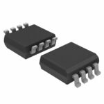 TC7WPN3125FK,LF(CT
The activity of extra discounts on wholesale prices is in full swing…
Please fill in your contact information and we will send you the latest wholesale price list.





