 ChipApex | Global Electronic Components Supplier
SEARCH
Search Product
Search Post
— IC芯片 | 连接器 | 传感器 | 被动器件 —
Search productSearch post
— IC芯片 | 连接器 | 传感器 | 被动器件 —
Consult the customer manager about the wholesale price.
consultation hotline:86-132-6715-2157
email:[email protected]
Contact the product manager for consultation. One-stop consultation is available.
Do you want a lower wholesale price? Please send us your inquiry and we will reply immediately.
The TC7WT125FU is a high-speed CMOS dual bus buffer fabricated with silicon gate technology. It operates within a supply voltage range of 4.5 V to 5.5 V and supports an operating temperature from -40°C to +85°C. The device features two non-inverting buffers with three-state outputs controlled by inputs G1 and G2. Key electrical parameters include a typical propagation delay of 13 ns at 5 V, symmetrical output drive capability of 6 mA minimum for both high and low states, and a maximum quiescent supply current of 2 μA at 25°C. Input thresholds are compatible with TTL levels.
Verify the specific ordering suffix and package marking against the manufacturer's latest documentation before procurement. Confirm that the component meets the required RoHS compliance standards for your region. Ensure the supplier provides traceability data consistent with Toshiba Semiconductor and Storage manufacturing records. Validate that the received units match the specified SM-8 package dimensions and pin configuration.
Select this component when a dual-channel buffer with three-state control is required for 5 V logic systems. It is suitable for designs needing TTL-compatible input thresholds and high noise immunity. Consider the 6 mA output drive capability for driving multiple LSTTL loads. Verify that the 4.5 V to 5.5 V supply voltage range aligns with the system power rails.
The TC7WT125FU belongs to the TC7WT series of high-speed CMOS logic devices manufactured by Toshiba Semiconductor and Storage. It is designed as a dual bus buffer in an SM-8 (SSOP) surface-mount package. This series focuses on providing LSTTL-equivalent speed with CMOS power efficiency, making it appropriate for general-purpose digital logic buffering in consumer and industrial electronics.
The TC7W125FU is a related variant offering a wider supply voltage range of 2 V to 6 V. Verify if the broader voltage tolerance or different drive characteristics of the TC7W125FU meet the specific design requirements before substituting.
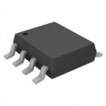 TC7WT125FU,LF
The activity of extra discounts on wholesale prices is in full swing…
Please fill in your contact information and we will send you the latest wholesale price list.





