 ChipApex | Global Electronic Components Supplier
SEARCH
Search Product
Search Post
— IC芯片 | 连接器 | 传感器 | 被动器件 —
Search productSearch post
— IC芯片 | 连接器 | 传感器 | 被动器件 —
Consult the customer manager about the wholesale price.
consultation hotline:86-132-6715-2157
email:[email protected]
Contact the product manager for consultation. One-stop consultation is available.
Do you want a lower wholesale price? Please send us your inquiry and we will reply immediately.
The TC7WT241FUTE12LF is a high-speed CMOS dual bus buffer featuring non-inverted, 3-state outputs. It operates within a supply voltage range of 4.5V to 5.5V and supports an operating temperature range from -40°C to 85°C. The device achieves a typical propagation delay of 13ns at VCC = 5V with a load capacitance of 15pF. Quiescent supply current is limited to a maximum of 2μA at 25°C. Output drive capability supports 15 LSTTL loads, with symmetrical output impedance providing a minimum source/sink current of 6mA.
Verify the specific ordering suffix TE12L corresponds to the required 8-SSOP package configuration. Confirm RoHS compliance status for environmental regulations. Ensure the supply voltage provided matches the 4.5V to 5.5V operational range. Validate that input signals remain within the specified DC voltage limits relative to VCC and GND.
Select this component when designing systems requiring dual-channel buffering with independent tri-state control. The device is suitable for applications needing TTL-compatible input thresholds without level shifting. Consider the 8-SSOP package constraints for PCB layout. Evaluate the 13ns propagation delay against system timing requirements under varying load conditions.
This part belongs to the TC7WT series of Toshiba CMOS digital integrated circuits. It utilizes silicon gate technology to achieve performance similar to LSTTL devices. The series focuses on providing high-speed switching capabilities combined with the low power characteristics inherent to CMOS design methodologies.
TC7WT125FU, LF serves as a parameter-equivalent substitute within the same manufacturer lineup.
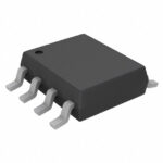 TC7WT241FUTE12LF
The activity of extra discounts on wholesale prices is in full swing…
Please fill in your contact information and we will send you the latest wholesale price list.





