 ChipApex | Global Electronic Components Supplier
SEARCH
Search Product
Search Post
— IC芯片 | 连接器 | 传感器 | 被动器件 —
Search productSearch post
— IC芯片 | 连接器 | 传感器 | 被动器件 —
Consult the customer manager about the wholesale price.
consultation hotline:86-132-6715-2157
email:[email protected]
Contact the product manager for consultation. One-stop consultation is available.
Do you want a lower wholesale price? Please send us your inquiry and we will reply immediately.
The TC9592XBG is a CMOS digital integrated circuit functioning as a DSI-to-LVDS bridge for automotive peripheral devices. It converts MIPI DSI video streams to LVDS signals for display panels, supporting up to 1600×1200 resolution at single-link and WUXGA (1920×1200) at dual-link. The device features a configurable 1- to 4-lane DSI receiver with a maximum bit rate of 1 Gbps per lane and an LVDS transmitter operating at pixel clocks up to 135 MHz. Power supplies include 1.2 V for DSI/LVDS PHY and core, and 1.8 V or 3.3 V for I/O. It includes an on-chip I2C Master controlled by the DSI link and supports power-saving states via ULPS signaling and a dedicated STBY pin.
Verify the specific ordering suffix against the manufacturer's official documentation to confirm package type and qualification grade. The TC9592XBG variant typically corresponds to the BGA49 package supporting single-link LVDS. Ensure the selected part matches the required AEC-Q100 Grade 3 qualification if intended for automotive applications, as this qualification is explicitly noted for the TC9593XBG model in the functional specification.
Select the TC9592XBG for designs requiring single-link LVDS output with a 5x5 mm BGA49 footprint. Choose the TC9593XBG if dual-link LVDS support for WUXGA resolutions is necessary, noting its larger BGA64 package. Confirm that the host processor supports MIPI DSI video mode and that the target display panel accepts LVDS input with compatible pixel formats such as RGB666 or RGB888.
The TC9592XBG serves as a successor to the TC358764XBG series, offering updated performance including higher DSI bit rates and reduced LVDS Tx power consumption. It is part of Toshiba's automotive peripheral device lineup designed to address PCIe interface shortages in modern vehicle architectures by facilitating high-speed communication between SoCs and display peripherals.
The TC358764XBG is identified as the predecessor chip. Designers migrating from the TC358764XBG should verify pin compatibility and register mapping differences, particularly regarding the new STBY pin functionality and updated power supply configurations specified in the TC9592XBG datasheet.
The TC9592XBG supports up to 1600×1200 24-bits per pixel resolution for single-link LVDS displays. For dual-link LVDS, it supports WUXGA (1920×1200) resolutions, though the TC9592XBG specifically is configured for single-link output.
A power-down state is achieved when the Reset signal is asserted, EXTCLK is not toggling, the STBY pin is low (0), and the DSI interface is in Ultra Low Power State (ULPS) drive.
No, the on-chip I2C Master function is controlled by the Host through the DSI link, and multi-master operation is not supported.
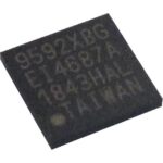 TC9592XBG(EL)
The activity of extra discounts on wholesale prices is in full swing…
Please fill in your contact information and we will send you the latest wholesale price list.






