 ChipApex | Global Electronic Components Supplier
SEARCH
Search Product
Search Post
— IC芯片 | 连接器 | 传感器 | 被动器件 —
Search productSearch post
— IC芯片 | 连接器 | 传感器 | 被动器件 —
Consult the customer manager about the wholesale price.
consultation hotline:86-132-6715-2157
email:[email protected]
Contact the product manager for consultation. One-stop consultation is available.
Do you want a lower wholesale price? Please send us your inquiry and we will reply immediately.
The TDA1519C is a Class-B dual output power amplifier available in 9-lead SIL or 20-lead HSOP packages. It delivers up to 22 W in Bridge-Tied Load (BTL) mode with a 4 Ω load, or 2 × 11 W in stereo configuration. The device operates on a supply voltage ranging from 6 V to 17.5 V. Key electrical parameters include a fixed closed-loop gain of 40 dB and a maximum total quiescent current of 80 mA. It features low DC output offset voltage and high ripple rejection.
Verify the specific package variant required, as the TDA1519C family includes distinct physical forms such as the 9-lead SIL (SOT131-2), surface-mount SIL (SOT354-1), and 20-lead HSOP (SOT397-1). Confirm that the selected part matches the intended mounting method and thermal dissipation strategy. Ensure compatibility with existing PCB footprints before procurement.
Select the TDA1519C when a robust Class-B amplifier with integrated protection is needed for single-supply applications. Choose the BTL configuration for higher power output into lower impedance loads, or stereo mode for independent channel control. Consider the 20-lead HSOP package if superior thermal performance via PCB soldering is required compared to the standard through-hole options.
This component belongs to the TDA151 series of power amplifiers manufactured by NXP Semiconductors. It is pin-compatible with the TDA1519B and TDA1519CSP variants, allowing for design flexibility across different packaging needs while maintaining identical electrical characteristics and functional behavior within the same product family.
The TDA1519B is a confirmed pin-compatible substitute within the same family. Verify that any replacement maintains the required package type (SIL or HSOP) and thermal resistance specifications to ensure proper heat dissipation and mechanical fit in the original application.
The M/SS pin controls both mute and standby modes. A voltage above 8.5 V enables normal operation, between 3.3 V and 6.4 V activates mute mode, and below 2 V engages standby mode.
The absolute maximum non-operating supply voltage is 30 V. The device is also protected against load dump conditions up to 45 V for durations of at least 50 ms.
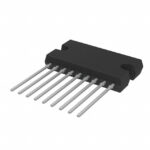 TDA1519C/N3C,112
The activity of extra discounts on wholesale prices is in full swing…
Please fill in your contact information and we will send you the latest wholesale price list.






