 ChipApex | Global Electronic Components Supplier
SEARCH
Search Product
Search Post
— IC芯片 | 连接器 | 传感器 | 被动器件 —
Search productSearch post
— IC芯片 | 连接器 | 传感器 | 被动器件 —
Consult the customer manager about the wholesale price.
consultation hotline:86-132-6715-2157
email:[email protected]
Contact the product manager for consultation. One-stop consultation is available.
Do you want a lower wholesale price? Please send us your inquiry and we will reply immediately.
The TDA1566 is a car audio power amplifier featuring two Bridge Tied Load (BTL) output stages realized in BCDMOS technology. It supports dual channel operation with 4 Ω or 2 Ω loads, or single channel configuration driving a 1 Ω load by paralleling outputs on the PCB. The device offers I²C-bus and non-I²C-bus control modes, enabling selectable gain settings of 26 dB and 16 dB per channel. Integrated diagnostic features include DC and AC load identification, speaker fault detection, and thermal pre-warning capabilities accessible via the I²C interface or dedicated pins.
Verify the specific ordering suffix to confirm package type and I²C address configuration. The TH version utilizes an HSOP24 package with four I²C addresses, while the J version uses a DBS27P package with two addresses. Ensure compatibility with existing board layouts regarding pin assignments and thermal requirements before finalizing procurement decisions.
Choose the TH version for designs requiring multiple I²C addresses or specific pin configurations compatible with the TDA8566TH1. Select the J version for applications needing fewer address bits or different physical packaging constraints. Consider the required load impedance and whether single channel high-power output or dual channel stereo operation best fits the system architecture.
This component belongs to NXP's portfolio of automotive audio power amplifiers designed for robust performance in vehicle environments. It complements other signal processing and microcontroller solutions by providing high-efficiency power delivery with integrated diagnostics. The device supports long-term supply plans to ensure stability for automotive manufacturing cycles.
The TH version is pin-compatible with the TDA8566TH1. Verify electrical specifications and pinout alignment when substituting this part. Ensure that any replacement maintains the same BCDMOS process characteristics and I²C communication protocols to avoid redesigning the control circuitry.
Connect the outputs of both BTL channels in parallel on the printed-circuit board. The input signal must be taken from channel 1, and the 1Ω select pin must be connected to VP.
The I²C bus provides access to DC and AC load detection results, clip detection levels, thermal pre-warning status, offset detection, and short-to-ground or short-to-supply faults for each channel.
Pop-free transitions are achieved by using the SVR capacitor for smooth start-up and shutdown. The output voltage tracks the SVR voltage, and gain increases gradually once the SVR voltage exceeds a specific threshold.
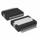 TDA1566TH/N2S,118
The activity of extra discounts on wholesale prices is in full swing…
Please fill in your contact information and we will send you the latest wholesale price list.






