 ChipApex | Global Electronic Components Supplier
SEARCH
Search Product
Search Post
— IC芯片 | 连接器 | 传感器 | 被动器件 —
Search productSearch post
— IC芯片 | 连接器 | 传感器 | 被动器件 —
Consult the customer manager about the wholesale price.
consultation hotline:86-132-6715-2157
email:[email protected]
Contact the product manager for consultation. One-stop consultation is available.
Do you want a lower wholesale price? Please send us your inquiry and we will reply immediately.
The TDA3653B/N2,112 is a vertical deflection and guard circuit designed for driving various deflection systems with peak-to-peak currents up to 1.5 A. It integrates a driver, output stage, thermal protection, flyback generator, voltage stabilizer, and guard circuit within a 9-lead SIL plastic package (SOT110B). The supply voltage range spans 10 V to 40 V, while the maximum supply voltage at pin 6 and peak output voltage during flyback are limited to 60 V. The device operates within a junction temperature range of -25 °C to +150 °C.
Verify component authenticity as this part number represents a legacy Philips product now under NXP USA Inc. The datasheet indicates the product status may be discontinued or obsolete; confirm availability through authorized distributors. Ensure the 9-SIL MPF package matches the design requirements for through-hole mounting on printed-circuit boards.
Select the TDA3653B/N2,112 for applications requiring a single-chip solution for vertical deflection drive up to 1.5 A. Ensure the supply voltage remains within 10 V to 40 V and that the flyback voltage at pin 5 does not exceed 60 V. Consider the thermal resistance of 10 K/W (junction to mounting base) for heat dissipation planning in the SOT110B package.
The TDA3653B is part of the TDA3653 family, which includes the TDA3653C variant. While the TDA3653B uses the 9-lead SIL plastic package (SOT110B), the TDA3653C utilizes a different 9-lead SIL plastic power package (SOT131). Both serve similar vertical deflection functions but differ in physical packaging and thermal characteristics.
The TDA3653C is a functional alternative within the same family, distinguished primarily by its SOT131 package instead of SOT110B. Verify pin compatibility and thermal performance differences before substitution. No other direct cross-model replacements are documented in the provided specifications.
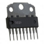 TDA3653B/N2,112
The activity of extra discounts on wholesale prices is in full swing…
Please fill in your contact information and we will send you the latest wholesale price list.






