 ChipApex | Global Electronic Components Supplier
SEARCH
Search Product
Search Post
— IC芯片 | 连接器 | 传感器 | 被动器件 —
Search productSearch post
— IC芯片 | 连接器 | 传感器 | 被动器件 —
Consult the customer manager about the wholesale price.
consultation hotline:86-132-6715-2157
email:[email protected]
Contact the product manager for consultation. One-stop consultation is available.
Do you want a lower wholesale price? Please send us your inquiry and we will reply immediately.
The TDA7256 is a Class AB fully protected bridge power amplifier designed for car radio applications. It features a Multiwatt11 package with 11 pins and supports an operating supply voltage range of 8V to 18V. The device delivers up to 30W output power into a 2Ω load, 26W into 3.2Ω, and 22W into 4Ω at 1kHz with 10% distortion. Key electrical characteristics include a quiescent drain current of 80-150mA, input resistance of 50kΩ, common mode rejection of 60dB, and supply voltage rejection of 45-60dB. Thermal protection activates at a junction temperature of 145°C.
Verify component authenticity through authorized STMicroelectronics distributors or certified partners. Confirm the specific ordering suffix matches the required packaging configuration. Ensure thermal management solutions align with the specified junction-to-case thermal resistance limits. Review datasheet revisions for any updates to absolute maximum ratings or electrical characteristics before finalizing procurement orders.
Select this component for high-current automotive audio designs requiring drive capability down to 2Ω loads. The differential input architecture is suitable for environments with significant electromagnetic interference. Evaluate the programmable turn-on delay requirements against the external capacitor values needed for the desired startup transient behavior. Ensure the Multiwatt11 package fits within the available chassis space and thermal dissipation constraints.
The TDA7256 belongs to STMicroelectronics' dedicated automotive audio amplifier portfolio. It utilizes advanced BCD technology to integrate high-voltage power stages with low-voltage control logic on a single chip. This integration allows for compact designs with minimal external components while maintaining robust performance in harsh automotive electrical environments.
Check for updated product line replacements such as the TDA7265 series. Verify pin compatibility and thermal performance metrics when substituting. Ensure that alternative devices maintain the same bridge configuration and short-circuit protection levels.
The delay time is determined by the external capacitors C9, C10, and C11 connected to the standby pin, following the formula: To = 800 * C10 + 600 * (C9 + C11) * (C10 / (C9 + C11 + 1)).
The device includes specific protection circuits designed to handle load dump voltage surges, preventing damage to the internal power stage during transient automotive electrical events.
No, the mute circuit acts at the preamplifier level and disables inputs without changing DC voltages. Combined with a soft reduction RC network, it ensures fully popless operation.
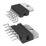 TDA7256
The activity of extra discounts on wholesale prices is in full swing…
Please fill in your contact information and we will send you the latest wholesale price list.





