 ChipApex | Global Electronic Components Supplier
SEARCH
Search Product
Search Post
— IC芯片 | 连接器 | 传感器 | 被动器件 —
Search productSearch post
— IC芯片 | 连接器 | 传感器 | 被动器件 —
Consult the customer manager about the wholesale price.
consultation hotline:86-132-6715-2157
email:[email protected]
Contact the product manager for consultation. One-stop consultation is available.
Do you want a lower wholesale price? Please send us your inquiry and we will reply immediately.
The TDA8351 is a DC-coupled vertical deflection circuit designed for 90° and 110° color deflection systems operating at field frequencies of 50 to 120 Hz. It functions as a highly efficient Class G output bridge, utilizing two supply voltages: VP (9–25 V) for scan voltage and VFB (up to 60 V) for flyback voltage. The device delivers a typical peak-to-peak output current of 3 A with a quiescent supply current of 30 mA. Key features include integrated thermal protection, short-circuit protection for output pins and to VP, and a guard signal output for blanking applications.
Verify the package type SIL9P (SOT131-2) and mounting method (Through Hole). Confirm that the ordering suffix 112 corresponds to the specific tape and reel or tube configuration required by your assembly process, as datasheet details on packaging quantities are not provided in the source material.
Select this component for applications requiring a DC-coupled vertical output stage with high efficiency. Ensure the design supports a dual-supply architecture with VP up to 25 V and VFB up to 60 V. Verify that the input driver provides symmetrical current signals compatible with the differential input requirements.
The TDA8351 belongs to the Philips/NXP family of specialized ICs for consumer electronics, specifically targeting CRT display vertical deflection. It is often used in conjunction with drivers such as the TDA9150, TDA9151B, TDA9160A, TDA9162, TDA8366, and TDA8376.
Public confirmed substitute part numbers are not available in the provided documentation.
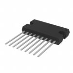 TDA8351/N6,112
The activity of extra discounts on wholesale prices is in full swing…
Please fill in your contact information and we will send you the latest wholesale price list.





