 ChipApex | Global Electronic Components Supplier
SEARCH
Search Product
Search Post
— IC芯片 | 连接器 | 传感器 | 被动器件 —
Search productSearch post
— IC芯片 | 连接器 | 传感器 | 被动器件 —
Consult the customer manager about the wholesale price.
consultation hotline:86-132-6715-2157
email:[email protected]
Contact the product manager for consultation. One-stop consultation is available.
Do you want a lower wholesale price? Please send us your inquiry and we will reply immediately.
The TDA8512J/N1,112 is a class-B power amplifier integrated circuit manufactured by NXP Semiconductors. It features four single-ended channels capable of delivering up to 13 W per channel into a 2 Ω load or two BTL channels providing 26 W into a 4 Ω load. The device operates within a supply voltage range of 6 V to 18 V and includes built-in thermal and short-circuit protection. It utilizes a 17-lead DBS17P plastic DIL-bent-SIL package designed for through-hole mounting in automotive and multimedia audio applications.
Verify component authenticity through authorized distribution channels as this part may be subject to obsolescence. Confirm that the specific ordering suffix matches the required package variant and compliance standards. Review the latest manufacturer documentation for any updates regarding lead-free status or material declarations before finalizing procurement plans.
Select this amplifier when designing systems requiring flexible channel configurations between single-ended and bridge-tied loads. Ensure the power supply can deliver sufficient current for peak outputs and that adequate heatsinking is provided given the thermal resistance characteristics. Verify input coupling capacitor values to maintain desired low-frequency response while minimizing switch-on delays.
This component belongs to the TDA851x series of power amplifiers from NXP Semiconductors. It shares architectural similarities with the TDA8510 and TDA8511 but offers distinct channel configuration options. The series is designed for robust performance in demanding audio environments, providing reliable amplification with minimal external component requirements.
Official substitutes include the TDA8510J and TDA8511J. Verify pin compatibility and electrical specifications against the original design requirements before substitution. Ensure that any replacement part meets the same thermal and voltage limiting values specified for the TDA8512J.
To avoid audible plops, the amplifier should be kept in mute mode for longer than 100 ms during switch-on. This allows the input capacitors at pins INV1, INV2, INV3, and INV4 to charge smoothly, preventing sudden DC shifts at the outputs.
Standby mode is activated by applying a low DC level between 0 V and 2 V to the MODE pin. In this state, power consumption reduces to less than 1.5 mW, and input/output pins enter a high-impedance floating condition.
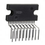 TDA8512J/N1,112
The activity of extra discounts on wholesale prices is in full swing…
Please fill in your contact information and we will send you the latest wholesale price list.






