 ChipApex | Global Electronic Components Supplier

SEARCH
Search Product
Search Post
— IC芯片 | 连接器 | 传感器 | 被动器件 —
Search productSearch post
— IC芯片 | 连接器 | 传感器 | 被动器件 —
Consult the customer manager about the wholesale price.
consultation hotline:86-132-6715-2157
email:[email protected]
Contact the product manager for consultation. One-stop consultation is available.
Do you want a lower wholesale price? Please send us your inquiry and we will reply immediately.
TDA8784HL/C5,118 is listed in the ADCs/DACs - Special Purpose range at ChipApex. The manufacturer field lists NXP USA Inc.. Its product description is IC ADC 10BIT 18M 48LQFP. Review the specifications below when checking this part for your BOM.
The TDA8784HL/C5,118 is a 10-bit analog-to-digital interface designed for CCD cameras. It integrates a correlated double sampling (CDS) circuit, an automatic gain control (AGC) amplifier, and a low-power 10-bit ADC with a reference regulator. The device supports sampling frequencies up to 18 MHz and features fully programmable bandwidths for CDS (4–120 MHz) and AGC (4–54 MHz). It operates on a 5 V analog supply and digital outputs compatible with 2.5 to 5.25 V logic levels. Key specifications include a typical power consumption of 483 mW and an AGC gain range of 4.5 to 34.5 dB.
Verify the ordering suffix against the manufacturer's documentation to confirm package type and tape/reel specifications. Ensure that the voltage requirements for VCCA, VCCD, and VCCO align with the system design, as the device supports separate analog and digital supplies. Confirm availability through authorized NXP Semiconductors distributors or verified electronic component suppliers.
Select this component for applications requiring high-speed digitization of CCD sensor signals with integrated signal conditioning. The device is suitable where space is constrained due to its single-chip integration of CDS, AGC, and ADC functions. Consider the 48-LQFP package dimensions and the need for separate analog and digital ground planes to minimize noise in sensitive imaging applications.
The TDA8784 series was originally developed by Philips Semiconductors, which later became NXP Semiconductors. The datasheet indicates it supersedes data from September 21, 1999, with the current specification dated October 23, 2002. This part represents a specialized interface solution for video imaging systems prevalent in the early 2000s.
Publicly confirmed substitute part numbers are not available in the provided source material. Designers should consult NXP Semiconductors for current equivalent products or verify pin-compatible alternatives based on specific application requirements.
The maximum clock frequency (fCLK) is 18 MHz, which corresponds to the maximum sampling rate.
The AGC gain is programmable from 4.5 dB to 34.5 dB in 0.1 dB steps via a 9-bit control input through the serial interface.
Yes, the digital outputs can operate with a supply voltage (VCCO) ranging from 2.5 V to 5.25 V, while the analog and main digital supplies (VCCA, VCCD) typically require 5 V.
Explore related parts through Data Acquisition, Integrated Circuits (ICs), all product categories, ChipApex homepage.
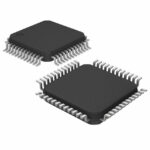 TDA8784HL/C5,118

The activity of extra discounts on wholesale prices is in full swing…
Please fill in your contact information and we will send you the latest wholesale price list.





