 ChipApex | Global Electronic Components Supplier
SEARCH
Search Product
Search Post
— IC芯片 | 连接器 | 传感器 | 被动器件 —
Search productSearch post
— IC芯片 | 连接器 | 传感器 | 被动器件 —
Consult the customer manager about the wholesale price.
consultation hotline:86-132-6715-2157
email:[email protected]
Contact the product manager for consultation. One-stop consultation is available.
Do you want a lower wholesale price? Please send us your inquiry and we will reply immediately.
The TDF8544J/N2,112 is an I2C-bus controlled quad Bridge-Tied Load (BTL) audio power amplifier designed for automotive applications. It utilizes a complementary DMOS output stage in an SOI-based BCD process to deliver high power with minimal distortion. The device operates at supply voltages as low as 6 V, ensuring seamless performance during engine start cycles. It features comprehensive diagnostics, including start-up load detection and thermal protection, housed in a 27-lead DBS27P plastic DIL-bent-SIL package.
Verify the specific ordering suffix and package variant when sourcing, as the TDF8544 series includes multiple pin configurations such as TH and SD. Confirm that the J/N2 designation matches the required DBS27P package type for your PCB layout. Ensure compatibility with your system's I2C voltage levels, as the device supports both 3.3 V and 5 V compliant modes.
Select this component for designs requiring integrated I2C control and extensive fault detection capabilities. It is suitable for environments where low-voltage operation during cranking is critical. Consider the DBS27P package for through-hole mounting requirements. Ensure adequate heatsinking is provided due to the high power dissipation characteristics of the BTL configuration.
This part belongs to the TDF8544 family of complementary quad BTL audio power amplifiers from NXP Semiconductors. The family is engineered using Silicon-On-Insulator (SOI) technology to prevent latch-up and ensure channel isolation. It serves as a modern replacement for older standalone amplifier solutions, offering enhanced diagnostic features and software compatibility with previous generations like the TDA8594.
The TDF8544 is software and hardware compatible with predecessor models TDA8594 and TDA8595. When replacing these older components, verify that the legacy mode pin connections are correctly configured if I2C communication is not utilized. Ensure that the new part's thermal management requirements are met within the existing enclosure design.
The amplifier uses a capacitor on the SVR pin to create a reference voltage that follows the supply voltage slowly. This prevents common mode ripple and ensures the DC input bias tracks the supply, avoiding audible plop noises even when the battery voltage drops to 6 V during cranking.
During start-up, the device performs load detection to identify open loads, shorted loads, or the presence of a separate booster amplifier. It also checks for shorts to ground or VP. These diagnostics are filtered to ignore disturbances from door slams or relay chatter.
Yes, the TDF8544 can operate in legacy mode by shorting the ADSEL pin to ground. In this mode, it functions without I2C communication, and the STB pin acts as a three-level control for stand-by, on, and mute states.
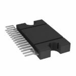 TDF8544J/N2,112
The activity of extra discounts on wholesale prices is in full swing…
Please fill in your contact information and we will send you the latest wholesale price list.





