 ChipApex | Global Electronic Components Supplier

SEARCH
Search Product
Search Post
— IC芯片 | 连接器 | 传感器 | 被动器件 —
Search productSearch post
— IC芯片 | 连接器 | 传感器 | 被动器件 —
Consult the customer manager about the wholesale price.
consultation hotline:86-132-6715-2157
email:[email protected]
Contact the product manager for consultation. One-stop consultation is available.
Do you want a lower wholesale price? Please send us your inquiry and we will reply immediately.
TE0715-04-51I33-A is listed in the Microcontrollers, Microprocessor, FPGA Modules range at ChipApex. The manufacturer field lists Trenz Electronic GmbH. Its product description is IC SOC MODULE 1GB DDR3L. Review the specifications below when checking this part for your BOM.
The Trenz Electronic TE0715-04-51I33-A is an industrial-grade System on Module (SoM) based on the Xilinx Zynq-7000 SoC, specifically the XC7Z030 variant. It integrates 1 GByte of 32-bit wide DDR3L SDRAM and 32 MBytes of Quad SPI Flash memory. The module features a Marvell Alaska 88E1512 Gigabit Ethernet PHY and a Microchip USB3320 high-speed ULPI transceiver for USB 2.0 connectivity. Powered by dual ARM Cortex-A9 processors, it provides rugged B2B connectors with 132 FPGA I/Os, 14 PS MIO pins, and four GTP/GTX high-performance transceiver lanes.
Verify the specific ordering suffix to confirm the processor speed grade and package type. Ensure the carrier board design supports the required power-on sequence and voltage levels for the HP banks if using the -30 variant. Confirm that the baseboard provides the necessary battery supply for the RTC functionality.
Select this module when high-performance processing is needed alongside programmable logic. The -30 variant offers more HP banks but requires strict adherence to 1.8V limits for those specific banks. Verify that the carrier board can accommodate the Samtec Razor Beam connectors and provides adequate cooling for the DC-DC converters under maximum load conditions.
This module belongs to the TE0715 family from Trenz Electronic, designed for Xilinx Zynq-7000 devices. It serves as a compact, industrial-grade building block for complex embedded designs. The -04-51I33-A designation indicates the specific configuration including the XC7Z030 processor, memory size, and temperature range specifications defined in the technical reference manual.
Direct replacements are limited within the same product line. Consider the TE0715-04-51I13-A if the lower-performance XC7Z015 SoC is sufficient for the application requirements. Both variants share the same mechanical footprint and peripheral layout, ensuring pin compatibility on the carrier board.
The default boot mode is Quad SPI, controlled by the MODE input signal on the B2B connector. A High or open state selects QSPI boot, while Low or ground selects SD Card boot.
A globally unique 48-bit node address compatible with EUI-48 specification is stored in the Microchip 24AA025E48 EEPROM at I2C slave address 0x50.
On the TE0715-xx-30 modules, Bank 34 consists of High Performance (HP) banks with a maximum voltage tolerance of 1.8V, unlike the HR banks on the -15 variant which support up to 3.3V.
Explore related parts through Embedded, Integrated Circuits (ICs), all product categories, ChipApex homepage.
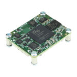 TE0715-04-51I33-A

The activity of extra discounts on wholesale prices is in full swing…
Please fill in your contact information and we will send you the latest wholesale price list.





