 ChipApex | Global Electronic Components Supplier
SEARCH
Search Product
Search Post
— IC芯片 | 连接器 | 传感器 | 被动器件 —
Search productSearch post
— IC芯片 | 连接器 | 传感器 | 被动器件 —
Consult the customer manager about the wholesale price.
consultation hotline:86-132-6715-2157
email:[email protected]
Contact the product manager for consultation. One-stop consultation is available.
Do you want a lower wholesale price? Please send us your inquiry and we will reply immediately.
The TFA9882UK is a mono, filter-free Class-D audio amplifier in a 9-bump WLCSP package (1.27 × 1.49 × 0.6 mm). It operates on a wide supply voltage range of 2.5 V to 5.5 V with a digital I2S interface. Output power reaches 3.4 W into 4 Ω at 5.0 V (THD=10%) and 2.7 W at THD=1%. Efficiency is 90% at 4 Ω/20 μH load. The device features low RF susceptibility, high supply voltage ripple rejection, and three gain settings (-3 dB, 0 dB, +3 dB).
Verify the specific ordering suffix 'N1,023' against official NXP documentation to confirm packaging or tape-and-reel specifications. Ensure the component matches the WLCSP9 footprint dimensions of 1.27 × 1.49 mm. Confirm that the digital supply voltage requirements align with your system's 1.8 V logic levels before integration.
Select this amplifier for applications requiring a compact mono Class-D solution with direct digital I2S connectivity. It is suitable for battery-powered devices due to its high efficiency and low quiescent power consumption. Consider the available gain settings and protection features when designing for varying supply voltages between 2.5 V and 5.5 V.
The TFA9882 is part of NXP's TFA series of digital audio amplifiers. It utilizes a Bridge-Tied Load (BTL) configuration with a 3-level PWM scheme, eliminating the need for external output filters. The device supports stereo applications by combining two units, allowing left/right channel selection via word select signals.
No public confirmed substitute part numbers are documented in the provided datasheet.
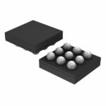 TFA9882UK/N1,023
The activity of extra discounts on wholesale prices is in full swing…
Please fill in your contact information and we will send you the latest wholesale price list.






