 ChipApex | Global Electronic Components Supplier
SEARCH
Search Product
Search Post
— IC芯片 | 连接器 | 传感器 | 被动器件 —
Search productSearch post
— IC芯片 | 连接器 | 传感器 | 被动器件 —
Consult the customer manager about the wholesale price.
consultation hotline:86-132-6715-2157
email:[email protected]
Contact the product manager for consultation. One-stop consultation is available.
Do you want a lower wholesale price? Please send us your inquiry and we will reply immediately.
The THC63LVDF84C-B is a deserializer IC from the THine Solutions LVDS series, designed for high-speed video data transmission. It converts four LVDS input channels into 28 CMOS/TTL output lines, supporting data rates up to 3.1Gbps. The device operates on a single 3V to 3.6V power supply and features a 56-TSSOP package with a width of 6.10mm. It supports pixel clock frequencies ranging from 8MHz to 112MHz and functions within an operating temperature range of -40°C to 85°C.
Verify the suffix 'B' against the manufacturer's official documentation to confirm specific pinout or electrical parameter variations compared to the standard THC63LVDF84C. Ensure compatibility with the system's voltage levels and clock requirements before integration. Cross-reference the 56-TSSOP footprint with PCB design files to prevent mechanical mismatches during assembly.
Select this component when a rising edge clocked LVDS receiver is required for resolutions up to SXGA at 112MHz. Compare against the THC63LVDR84C if falling edge timing is preferred instead. Ensure the application environment stays within the specified -40°C to 85°C temperature range and that the 3V to 3.6V supply rail is stable to maintain signal integrity across the 28 output lines.
This part belongs to the THine Solutions THC63LVD family of LVDS transceivers, widely used in consumer electronics for connecting host processors to LCD panels. The 'F' designation typically indicates a specific package variant or revision within the R84 series, while the '-B' suffix denotes a manufacturing lot or minor specification update defined by the original equipment manufacturer.
THC63LVDF84C is a direct functional equivalent. THC63LVDR84C serves as an alternative if falling edge clocking is acceptable rather than rising edge.
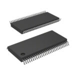 THC63LVDF84C-B
The activity of extra discounts on wholesale prices is in full swing…
Please fill in your contact information and we will send you the latest wholesale price list.





