 ChipApex | Global Electronic Components Supplier
SEARCH
Search Product
Search Post
— IC芯片 | 连接器 | 传感器 | 被动器件 —
Search productSearch post
— IC芯片 | 连接器 | 传感器 | 被动器件 —
Consult the customer manager about the wholesale price.
consultation hotline:86-132-6715-2157
email:[email protected]
Contact the product manager for consultation. One-stop consultation is available.
Do you want a lower wholesale price? Please send us your inquiry and we will reply immediately.
The THC63LVDR84C is a deserializer integrated circuit manufactured by THine Solutions, Inc., designed for high-speed serial data transmission. It converts four LVDS input channels into twenty-eight CMOS/TTL output lines. The device supports a maximum data rate of 3.1Gbps and operates with a supply voltage range of 3V to 3.6V. It is housed in a 56-TSSOP package with dimensions of 0.240 inches (6.10mm) width. The component functions within an ambient temperature range of -40°C to 85°C and complies with RoHS3 standards.
Verify the specific suffix designation when ordering, as variants such as THC63LVDR84C-B exist with identical electrical parameters but potentially different packaging or manufacturing lot attributes. Confirm the 56-TSSOP package requirement matches the target PCB footprint. Ensure the design supports the 3V to 3.6V supply rail and accommodates the specified operating temperature range for the intended environment.
Select this component when a 4-to-28 channel deserialization ratio is required for LVDS-based display interfaces. It is suitable for designs needing support for pixel clocks up to 160MHz. Compare against the THC63LVDF84C if a different clock edge triggering or pinout configuration is preferred, as both belong to the same functional family but may differ in specific timing characteristics or package availability.
This part belongs to the THine Solutions THC63LVDR series of LVDS receivers. It serves as the receiving end counterpart to serializers like the THC63LVDM83D. The series is widely used in consumer electronics and industrial displays requiring reliable, low-noise digital video transmission over short distances using standard LVDS cabling and connectors.
The THC63LVDF84C is documented as a parameter-equivalent substitute. Verify pin compatibility and clock edge specifications before swapping, as suffix variations may indicate differences in trigger edges or packaging revisions despite identical core functionality.
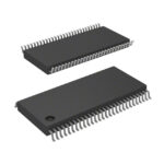 THC63LVDR84C
The activity of extra discounts on wholesale prices is in full swing…
Please fill in your contact information and we will send you the latest wholesale price list.






