 ChipApex | Global Electronic Components Supplier
SEARCH
Search Product
Search Post
— IC芯片 | 连接器 | 传感器 | 被动器件 —
Search productSearch post
— IC芯片 | 连接器 | 传感器 | 被动器件 —
Consult the customer manager about the wholesale price.
consultation hotline:86-132-6715-2157
email:[email protected]
Contact the product manager for consultation. One-stop consultation is available.
Do you want a lower wholesale price? Please send us your inquiry and we will reply immediately.
The THCV220 is a receiver LSI designed to convert V-by-One HS input signals into 32-bit LVCMOS output signals. It supports a maximum effective data rate of 3.0 Gbps per lane, enabling the reception of 720p/60Hz video signals with 30-bit color depth. The device operates on a supply voltage ranging from 2.5V to 3.3V and is housed in a QFN64 package. It functions within an operating temperature range of -40°C to 85°C and includes AEC-Q100 ESD protection features.
Verify the specific revision level and packaging options available from authorized distributors. Confirm that the required V-by-One HS source components, such as the THCV219 or THCV233, are compatible with your system design. Ensure that the power supply rails meet the specified 2.5V to 3.3V requirements for stable operation.
Select this component when a V-by-One HS to LVCMOS conversion is required for 720p video applications. Consider the 32-bit output width if higher bandwidth efficiency is needed compared to 24-bit alternatives. Verify thermal management capabilities for the QFN64 package within the target operating temperature range.
The THCV220 serves as a bridge between high-speed serial video interfaces and parallel digital logic. It is part of a family of display interface solutions, often paired with specific transmitter ICs to ensure signal integrity across short to medium distances in consumer and automotive electronics.
Check for direct pin-to-pin replacements within the THine Solutions portfolio. Evaluate alternative LVCMOS receivers if V-by-One HS compatibility is not strictly required. Verify electrical characteristics against existing design constraints before substitution.
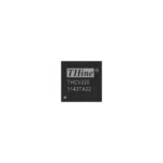 THCV220
The activity of extra discounts on wholesale prices is in full swing…
Please fill in your contact information and we will send you the latest wholesale price list.





