 ChipApex | Global Electronic Components Supplier
SEARCH
Search Product
Search Post
— IC芯片 | 连接器 | 传感器 | 被动器件 —
Search productSearch post
— IC芯片 | 连接器 | 传感器 | 被动器件 —
Consult the customer manager about the wholesale price.
consultation hotline:86-132-6715-2157
email:[email protected]
Contact the product manager for consultation. One-stop consultation is available.
Do you want a lower wholesale price? Please send us your inquiry and we will reply immediately.
The THCV234 is a signal conversion LSI designed to translate 32-bit V-by-One HS input signals into LVDS output signals. It supports a maximum effective data rate of 3.36 Gbps per lane for its two-lane V-by-One HS input interface. The device provides five channels of LVDS data output, accommodating configurations such as 24-bit or 32-bit pixel data depending on the lane setup. It operates with an LVDS input clock frequency ranging from 9 MHz to 105 MHz and utilizes a QFN48 package.
Verify the specific datasheet version and pinout compatibility before integration. Confirm that the target system supports the required 1.8V or 3.3V power supply levels. Ensure the PCB layout accommodates the QFN48 package dimensions and thermal requirements for reliable operation at specified data rates.
Select this component when interfacing V-by-One HS sources with LVDS-based displays. Verify that the source device can drive the required differential signaling standards. Consider the maximum clock frequency limits of the downstream LVDS receivers to ensure signal integrity across the full operational range.
THine Solutions specializes in high-speed serial interface technologies for display applications. The THCV234 belongs to a family of bridge chips that facilitate connectivity between modern high-bandwidth video sources and traditional parallel display interfaces, enabling seamless integration in complex visual systems.
Publicly confirmed substitute part numbers are not available in the provided documentation. Evaluate alternative bridge ICs based on matching V-by-One HS input capabilities and LVDS output channel counts.
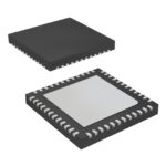 THCV234
The activity of extra discounts on wholesale prices is in full swing…
Please fill in your contact information and we will send you the latest wholesale price list.





