 ChipApex | Global Electronic Components Supplier
SEARCH
Search Product
Search Post
— IC芯片 | 连接器 | 传感器 | 被动器件 —
Search productSearch post
— IC芯片 | 连接器 | 传感器 | 被动器件 —
Consult the customer manager about the wholesale price.
consultation hotline:86-132-6715-2157
email:[email protected]
Contact the product manager for consultation. One-stop consultation is available.
Do you want a lower wholesale price? Please send us your inquiry and we will reply immediately.
The TLV320DAC3202 is a low-power, high-fidelity stereo headset integrated circuit featuring an I2S input DAC and Class-G amplifier. It operates on a single battery supply (AVDD: 2.3 V to 4.8 V) with digital I/O voltage (DVDD: 1.65 V to 1.95 V). The device delivers 100-dBA SNR with 6.5 mW quiescent power dissipation. It supports sampling rates of 8 kHz to 48 kHz and data widths of 16-, 20-, 24-, and 32-bit. The package is a WCSP (YZJ), measuring 2 mm x 2.5 mm.
Verify the specific suffix 'JR' indicates tape and reel packaging containing 3000 units per reel. Confirm the YZJ package footprint requirements against the datasheet diagrams, as it does not conform to standard YZJ footprints. Ensure system design accounts for the 2 mm x 2.5 mm WCSP dimensions and appropriate decoupling capacitors for AVDD, DVDD, and HSVDD rails.
Select this component for space-constrained portable applications requiring direct battery operation without external negative rails. The internal charge pump eliminates the need for complex power management circuits. Verify that the host processor can provide the required I2S clock signals (BCLK/WCLK) and that the I2C interface pull-up resistors are correctly sized for the desired communication speed.
This part belongs to Texas Instruments' dedicated headset codec family designed for mobile handsets. Unlike general-purpose audio codecs, it integrates the headphone amplifier directly with the DAC to minimize board space. The WCSP package allows for ultra-compact designs suitable for modern slim-profile mobile devices where traditional QFN packages would be too large.
TLV320DAC3202CYZJT
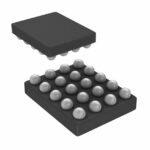 TLV320DAC3202CYZJR
The activity of extra discounts on wholesale prices is in full swing…
Please fill in your contact information and we will send you the latest wholesale price list.





