 ChipApex | Global Electronic Components Supplier

SEARCH
Search Product
Search Post
— IC芯片 | 连接器 | 传感器 | 被动器件 —
Search productSearch post
— IC芯片 | 连接器 | 传感器 | 被动器件 —
Consult the customer manager about the wholesale price.
consultation hotline:86-132-6715-2157
email:[email protected]
Contact the product manager for consultation. One-stop consultation is available.
Do you want a lower wholesale price? Please send us your inquiry and we will reply immediately.
TLV5613CDWR is listed in the Digital To Analog Converters range at ChipApex. The manufacturer field lists Texas Instruments. Its product description is IC DAC 12BIT V-OUT 20SOIC. Review the specifications below when checking this part for your BOM.
The TLV5613CDWR is a 12-bit voltage output digital-to-analog converter (DAC) featuring an 8-bit microcontroller-compatible parallel interface. It operates on a single supply ranging from 2.7 V to 5.5 V with separate analog and digital power pins. The device utilizes a resistor-string architecture buffered by a rail-to-rail x2 gain output stage. Key electrical parameters include ±0.4 LSB differential nonlinearity (DNL), ±1.5 LSB integral nonlinearity (INL), and a programmable settling time of 1 µs in fast mode or 3.5 µs in slow mode. Power consumption is 4.2 mW in fast mode, 1.2 mW in slow mode, and 50 nW in power-down mode.
Verify the 'R' suffix indicates tape-and-reel packaging rather than tube packaging when sourcing this specific part number. Confirm the operating temperature range matches the 'C' designation (0°C to 70°C). Ensure the component source provides valid traceability documentation consistent with Texas Instruments production standards.
Select this component for designs requiring a 12-bit resolution with a parallel interface. Consider the separate AVDD and DVDD pins if noise isolation is required. Evaluate the fast versus slow mode requirements based on system settling time constraints and available power budget.
This device belongs to the TLV5613 family of 12-bit CMOS DACs manufactured by Texas Instruments. The CDWR variant specifically denotes the commercial temperature grade housed in a SOIC-20 package and supplied in a tape-and-reel format for automated assembly processes.
Compatible alternatives within the same series include the TLV5613IDWR for industrial temperature ranges. Other pin-compatible options may exist but require verification of interface timing and electrical specifications against the original design requirements.
Settling time is controlled via the SPD bit in the control register or the physical SPD pin. Setting it to logic high enables fast mode (1 µs), while logic low enables slow mode (3.5 µs).
The reference input voltage can range from ground up to AVDD minus 1.5 V. Exceeding this limit may cause clipping of the transfer function due to the x2 output buffer gain.
Yes, the DAC update can be synchronized using the LDAC pin. Alternatively, asynchronous updates are possible by controlling the RLDAC bit in the control register.
Explore related parts through Data Acquisition, Integrated Circuits (ICs), all product categories, ChipApex homepage.
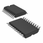 TLV5613CDWR

The activity of extra discounts on wholesale prices is in full swing…
Please fill in your contact information and we will send you the latest wholesale price list.






