 ChipApex | Global Electronic Components Supplier

SEARCH
Search Product
Search Post
— IC芯片 | 连接器 | 传感器 | 被动器件 —
Search productSearch post
— IC芯片 | 连接器 | 传感器 | 被动器件 —
Consult the customer manager about the wholesale price.
consultation hotline:86-132-6715-2157
email:[email protected]
Contact the product manager for consultation. One-stop consultation is available.
Do you want a lower wholesale price? Please send us your inquiry and we will reply immediately.
TLV5619QDWR is listed in the Digital To Analog Converters range at ChipApex. The manufacturer field lists Texas Instruments. Its product description is IC DAC 12BIT V-OUT 20SOIC. Review the specifications below when checking this part for your BOM.
The TLV5619QDWR is a 12-bit, single-channel voltage-output digital-to-analog converter (DAC) from Texas Instruments. It operates on a single supply ranging from 2.7 V to 5.5 V and features a microprocessor-compatible parallel interface with double-buffered data inputs. The device utilizes a resistor-string architecture and includes an internal power-on reset. Its output is buffered by a rail-to-rail amplifier with Class A characteristics, providing a gain of x2. Key electrical specifications include ±0.4 LSB differential nonlinearity, ±1.5 LSB integral nonlinearity, and a typical settling time of 1 µs. Power consumption is 8 mW at 5 V and 4.3 mW at 3 V, reducible to 50 nW in power-down mode.
Verify the specific suffix 'Q' indicates automotive qualification requirements before procurement. Confirm the 'DW' package designation matches the required SOIC-20 footprint. Ensure the operating temperature range aligns with system constraints. Check current production status as availability may vary. Validate RoHS compliance details against local regulatory standards.
Select this component when a high-resolution 12-bit DAC with a parallel interface is required. Consider the TLV5619QDWR for applications needing low power consumption and fast settling times. Evaluate the need for automotive-grade reliability if operating in harsh environments. Compare against serial interface alternatives if pin count reduction is critical.
The TLV5619 belongs to the TLV5619 series of 12-bit DACs. Variants include industrial grade parts like TLV5619IDWR and commercial grade parts like TLV5619CDWR. The Q-series variant specifically targets automotive applications, offering extended temperature ranges and enhanced reliability compared to standard industrial versions.
Direct replacements within the same family include TLV5619IDWR for industrial temperature ranges. For automotive contexts, verify compatibility with other qualified variants in the series. Cross-reference pinouts and electrical specifications to ensure functional equivalence without redesigning the host circuitry.
The reference voltage applied to the REFIN terminal must not exceed VDD minus 1.5 V. For a 5-V supply, this limits the reference to approximately 3.5 V, though typical operation uses lower values like 2.048 V.
Setting the PD pin low disables all buffer amplifier voltages, reducing the supply current to approximately 50 nW. This mode significantly lowers power consumption during idle periods.
The TLV5619QDWR provides a unipolar voltage output. The output range extends from ground up to nearly the full-scale voltage determined by the reference input.
Explore related parts through Data Acquisition, Integrated Circuits (ICs), all product categories, ChipApex homepage.
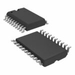 TLV5619QDWR

The activity of extra discounts on wholesale prices is in full swing…
Please fill in your contact information and we will send you the latest wholesale price list.





