 ChipApex | Global Electronic Components Supplier

SEARCH
Search Product
Search Post
— IC芯片 | 连接器 | 传感器 | 被动器件 —
Search productSearch post
— IC芯片 | 连接器 | 传感器 | 被动器件 —
Consult the customer manager about the wholesale price.
consultation hotline:86-132-6715-2157
email:[email protected]
Contact the product manager for consultation. One-stop consultation is available.
Do you want a lower wholesale price? Please send us your inquiry and we will reply immediately.
The TMA164S-L is a Triac (Bidirectional Triode Thyristor) from the TMA16xS Series manufactured by Sanken Electric USA Inc. It features a Peak Repetitive Off-State Voltage (VDRM) of 400 V and a Peak Non-Repetitive Off-State Voltage (VDSM) of 500 V. The device supports an RMS On-State Current (IT(RMS)) of 16 A at a case temperature of 66°C, with a Surge On-State Current (ITSM) of 160 A for 50 Hz full cycle sine waves. It utilizes a 3-pin SIP (TO-220F) package with a junction-to-case thermal resistance of 3.3 °C/W. The isolation voltage between lead and case is 1800 V AC RMS applied for 1 minute.
Verify component authenticity through official manufacturer channels or authorized distributors. Confirm that the specific part number matches the required electrical ratings, particularly the 400 V off-state voltage. Ensure handling procedures adhere to electrostatic discharge precautions during storage and installation to maintain device integrity.
Select this component for AC power control circuits requiring 16 A continuous current capability. Verify that the application operates within the specified junction temperature range of -40°C to 125°C. Ensure adequate heatsinking is provided to maintain the case temperature at or below 66°C for rated current operation. Consider the 1800 V isolation voltage for safety-critical designs.
The TMA164S-L belongs to the TMA16xS series of Triacs produced by Sanken Electric USA Inc. This series is characterized by robust construction and enhanced isolation capabilities. The 'S' suffix indicates the specific packaging type, while the 'L' denotes the lead configuration variant within the SIP form factor.
Public confirmed substitute part numbers are not available in the provided documentation. Designers should consult manufacturer resources for equivalent components if replacement is necessary.
The peak non-repetitive surge on-state current (ITSM) is 160 A for a 50 Hz full cycle sine wave with an initial junction temperature of 125°C.
Pin 3 is designated as the Gate (G) control terminal. Pin 1 is the Main Terminal 1 (T1), referenced to the gate, and Pin 2 is the Main Terminal 2 (T2).
The critical commutation dv/dt ((dv/dt)c) is specified as 10 V/μs at a junction temperature of 125°C, with VD = 400 V, (di/dt)c = –8 A/ms, and ITP = 2 A.
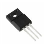 TMA164S-L

The activity of extra discounts on wholesale prices is in full swing…
Please fill in your contact information and we will send you the latest wholesale price list.





