 ChipApex | Global Electronic Components Supplier
SEARCH
Search Product
Search Post
— IC芯片 | 连接器 | 传感器 | 被动器件 —
Search productSearch post
— IC芯片 | 连接器 | 传感器 | 被动器件 —
Consult the customer manager about the wholesale price.
consultation hotline:86-132-6715-2157
email:[email protected]
Contact the product manager for consultation. One-stop consultation is available.
Do you want a lower wholesale price? Please send us your inquiry and we will reply immediately.
The TMUX1308APWR is a single-channel, 8:1 bidirectional analog multiplexer from Texas Instruments, housed in a 16-pin TSSOP package. It operates on a single supply voltage ranging from 1.62V to 5.5V. The device features an internal injection current control mechanism that eliminates the need for external protection diodes or resistors, allowing signals to exceed the supply voltage without affecting the enabled path. Key electrical parameters include a maximum on-resistance of 195 Ohms at 5V, a bandwidth of 500 MHz, and off-isolation of -90 dB at 1 MHz. It supports rail-to-rail signal operation and includes fail-safe logic for control pins.
Verify the specific ordering suffix 'PW' corresponds to the TSSOP-16 package with a 4.4mm body width. Confirm the component meets RoHS compliance requirements for your assembly process. Ensure the design accommodates the thermal dissipation characteristics specified for the TSSOP footprint under maximum operating temperatures.
Select this component when high-impedance load switching is required without external protection networks. The 1.8V logic compatibility simplifies interface with low-voltage microcontrollers. Consider the 195 Ohm on-resistance limit for signal integrity requirements at higher frequencies compared to lower resistance alternatives.
This part belongs to the TMUX13xxA family of CMOS multiplexers optimized for high-impedance loads. It is functionally similar to industry-standard 4051, 4851, and 1308 devices but offers enhanced protection features. The 'A' designation indicates the inclusion of internal injection current control capabilities not present in earlier generations.
Pin-compatible replacements include standard 4051, 4851, and 1308 multiplexers. Verify that substitute components can handle the same voltage excursions and leakage specifications if external protection circuits are omitted.
No, the device features internal injection current control that eliminates the need for external diode and resistor networks typically used to protect the switch and keep input signals within the supply voltage.
The device incorporates fail-safe logic that allows voltages on the control pins (EN, A0, A1, A2) to be applied before the supply pin, protecting the device from potential damage during power-up sequences.
Yes, signals on disabled or enabled signal paths can exceed the supply voltage. Disabled channels with voltages above VDD are prevented from affecting the signal of the enabled signal path.
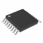 TMUX1308APWR
The activity of extra discounts on wholesale prices is in full swing…
Please fill in your contact information and we will send you the latest wholesale price list.





