 ChipApex | Global Electronic Components Supplier
SEARCH
Search Product
Search Post
— IC芯片 | 连接器 | 传感器 | 被动器件 —
Search productSearch post
— IC芯片 | 连接器 | 传感器 | 被动器件 —
Consult the customer manager about the wholesale price.
consultation hotline:86-132-6715-2157
email:[email protected]
Contact the product manager for consultation. One-stop consultation is available.
Do you want a lower wholesale price? Please send us your inquiry and we will reply immediately.
The TMUX1308QPWRQ1 is an automotive-grade, single-channel 8:1 CMOS multiplexer switch manufactured by Texas Instruments. It operates on a single supply voltage ranging from 1.62 V to 5.5 V and supports bidirectional analog and digital signals between ground and the supply rail. The device features a maximum on-resistance of 195 Ohms with a channel-to-channel matching of 7 Ohms. Key electrical parameters include a -3dB bandwidth of 500 MHz, typical off-isolation of -110 dB, and a propagation delay of 30 ns. Switching times are specified at a maximum of 32 ns for turn-on and 40 ns for turn-off. It is housed in a 16-TSSOP package and complies with AEC-Q100 standards for automotive applications.
Verify the specific suffix 'QPWRQ1' corresponds to the TSSOP-16 package and automotive grade qualification. Confirm AEC-Q100 certification status for your target environment. Check RoHS compliance details as indicated in official documentation. Ensure the ordering part number matches the required tape and reel specifications for surface mount assembly processes.
Select this component when an 8:1 multiplexing configuration is required in a compact 16-pin package. The 195 Ohm on-resistance suits general-purpose signal switching rather than high-current applications. The 500 MHz bandwidth supports high-frequency signal integrity needs. Verify that the 1.62 V minimum supply voltage aligns with the system's power architecture.
This device belongs to the TMUX13xx-Q1 family of CMOS multiplexers designed for automotive reliability. It serves as a direct pin-compatible replacement for industry-standard 4051 and 4851 multiplexers. The Q1 designation indicates adherence to automotive quality and reliability standards, distinguishing it from commercial-grade variants in the same series.
The TMUX1308DYYRQ1 offers a similar function in a SOT-23-THIN-16 package. The TMUX1308AQDYYRQ1 provides comparable performance in a thin SOT-23 form factor. Verify pinout compatibility and package dimensions before substituting these alternatives in existing designs.
Yes, the control inputs (Ax) can withstand up to 5.5 V regardless of the applied supply voltage.
The maximum off-state leakage current (IS(off)) is typically 1 nA.
Yes, the source (Sx) and drain (Dx) pins support bidirectional analog and digital signals from ground to VDD.
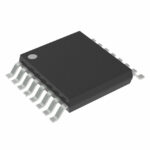 TMUX1308QPWRQ1
The activity of extra discounts on wholesale prices is in full swing…
Please fill in your contact information and we will send you the latest wholesale price list.





