 ChipApex | Global Electronic Components Supplier
SEARCH
Search Product
Search Post
— IC芯片 | 连接器 | 传感器 | 被动器件 —
Search productSearch post
— IC芯片 | 连接器 | 传感器 | 被动器件 —
Consult the customer manager about the wholesale price.
consultation hotline:86-132-6715-2157
email:[email protected]
Contact the product manager for consultation. One-stop consultation is available.
Do you want a lower wholesale price? Please send us your inquiry and we will reply immediately.
The TMUX1309APWR is a general-purpose CMOS multiplexer featuring two independent 4:1 channels in a 16-pin TSSOP package. It supports bidirectional analog and digital signals with a supply voltage range of 1.62V to 5.5V. Key electrical parameters include an on-resistance maximum of 195 Ohms at 5V, off-isolation of -90dB at 1MHz, and crosstalk of -90dB at 1MHz. The device operates within a temperature range of -40°C to +125°C, drawing a maximum supply current of 1µA.
Verify the specific ordering suffix 'PW' corresponds to the TSSOP-16 package configuration required for your PCB layout. Confirm that the component meets RoHS compliance standards for your manufacturing process. Ensure the design accommodates the specified thermal dissipation limits for the selected operating environment.
Select this component when differential signal routing is required due to its dual-channel architecture. Verify that the 195 Ohm on-resistance meets the signal integrity requirements of the high-impedance loads. Ensure the 1.8V logic compatibility aligns with the system's control voltage levels.
This part belongs to the TMUX13xxA family of low-voltage multiplexers optimized for high-impedance loads. It serves as a pin-compatible replacement for industry-standard 4052, 4852, and 1309 multiplexers, facilitating direct upgrades in existing designs without requiring schematic modifications.
Pin-compatible alternatives include the TMUX1308A for single-ended applications. Other standard replacements are the 4052, 4852, and 1309 multiplexers. Verify functional equivalence regarding injection current handling and logic thresholds before substitution.
The internal injection current control circuitry allows signals on disabled or enabled paths to exceed VDD without affecting the enabled signal path or damaging the device.
It protects the device from potential damage by allowing voltages on the control pins (EN, A0, A1) to be applied before the supply voltage is present.
No, the device does not have an internal diode path to the supply pin, which eliminates the risk of providing unintended power to the supply rail.
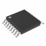 TMUX1309APWR
The activity of extra discounts on wholesale prices is in full swing…
Please fill in your contact information and we will send you the latest wholesale price list.





