 ChipApex | Global Electronic Components Supplier
SEARCH
Search Product
Search Post
— IC芯片 | 连接器 | 传感器 | 被动器件 —
Search productSearch post
— IC芯片 | 连接器 | 传感器 | 被动器件 —
Consult the customer manager about the wholesale price.
consultation hotline:86-132-6715-2157
email:[email protected]
Contact the product manager for consultation. One-stop consultation is available.
Do you want a lower wholesale price? Please send us your inquiry and we will reply immediately.
The TMUX1309AQPWRQ1 is an automotive-grade, bidirectional CMOS multiplexer featuring a 4:1 configuration with two differential channels. It operates on a single supply voltage ranging from 1.62 V to 5.5 V and supports rail-to-rail signal paths. The device incorporates internal injection current control to protect switches without external components. Key electrical parameters include a maximum on-resistance of 195 Ohms at 5 V, a typical off-isolation of -110 dB at 100 kHz, and a bandwidth up to 500 MHz. It utilizes a 16-pin TSSOP package and meets AEC-Q100 Grade 1 standards for operation between -40°C and +125°C.
Verify that the ordering suffix matches the required package type and temperature grade. Confirm the specific revision level against the manufacturer's latest documentation to ensure compatibility with functional safety requirements. Check RoHS compliance status as indicated in the official datasheet specifications.
Select this component when designing for high-impedance loads requiring bidirectional switching within a 5V automotive environment. Ensure the application benefits from the integrated injection current control to minimize external circuit complexity. Verify that the 1.8V logic thresholds align with the system's microcontroller output levels.
This part belongs to the TMUX13xxA-Q1 family of general-purpose CMOS multiplexers designed specifically for automotive applications. It serves as a differential channel variant alongside the single-ended TMUX1308A-Q1. The series is characterized by its robust protection features and direct replacement capability for legacy standard logic families.
Direct pin-compatible replacements include the TMUX1309DYYR and TMUX1309BQBR. Non-automotive equivalents such as the TMUX1209PWR offer lower on-resistance but lack AEC-Q100 qualification and injection current control.
The internal injection current control circuitry allows signals on disabled or enabled paths to exceed the supply voltage without affecting the active signal path or damaging the device.
Fail-safe logic protects the device from potential damage by allowing voltages on the control pins to be applied before the voltage is applied to the power supply pin.
No, the device does not have an internal diode path to the VDD pin, which prevents unintended power delivery to the supply rail or damage to connected components.
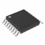 TMUX1309AQPWRQ1
The activity of extra discounts on wholesale prices is in full swing…
Please fill in your contact information and we will send you the latest wholesale price list.





