 ChipApex | Global Electronic Components Supplier

SEARCH
Search Product
Search Post
— IC芯片 | 连接器 | 传感器 | 被动器件 —
Search productSearch post
— IC芯片 | 连接器 | 传感器 | 被动器件 —
Consult the customer manager about the wholesale price.
consultation hotline:86-132-6715-2157
email:[email protected]
Contact the product manager for consultation. One-stop consultation is available.
Do you want a lower wholesale price? Please send us your inquiry and we will reply immediately.
TP3054WM-X/63 is listed in the Codecs range at ChipApex. The manufacturer field lists Texas Instruments. Its product description is IC FILTER ENHANCE INTERFC 16SOIC. Review the specifications below when checking this part for your BOM.
The TP3054WM-X/63 is a monolithic PCM CODEC/filter combo fabricated using TI's microCMOS process. It operates on ±5V supplies and supports μ-law encoding with a 16-pin package. The device integrates an input gain adjust amplifier, active RC pre-filter, switched-capacitor band-pass filter (200 Hz to 3400 Hz), companding coder, expanding decoder, low-pass filter with sin x/x correction, and a single-ended power amplifier. It requires master clocks of 1.536 MHz, 1.544 MHz, or 2.048 MHz and bit clocks from 64 kHz to 2.048 MHz. Typical active power consumption is 50 mW, while standby mode consumes approximately 3 mW.
Verify the specific suffix 'X' indicates extended temperature range operation (-40°C to +85°C) as defined by Texas Instruments. Confirm the '/63' designation corresponds to the tape and reel packaging format required for automated assembly processes. Cross-reference the datasheet revision SNOSBY2C to ensure compatibility with current design specifications.
Select this component when designing systems requiring integrated μ-law PCM encoding and decoding with minimal external passive components. Ensure the application utilizes a ±5V power supply architecture. Verify that the available master clock frequencies align with the synchronous or asynchronous timing requirements of the host processor.
This part belongs to the TP3054-X and TP3057-X Extended Temperature Serial Interface CODEC/Filter COMBO Family. The TP3054 variant specifically implements μ-law coding conventions, whereas the TP3057 variant utilizes A-law coding. Both share identical architectural features and pinouts but differ in their digital encoding standards.
TP3057WM-X/63: Functionally similar but uses A-law encoding instead of μ-law.
The device supports both short and long frame sync pulses. Short mode uses a pulse width of one bit clock period, while long mode requires three or more bit clock periods. The device automatically senses the pulse width upon power initialization.
The precision voltage reference provides an input overload level (tMAX) of nominally 2.5V peak at the GSX output pin.
Yes, separate transmit and receive master clocks can be applied. However, for best performance, MCLKR should be synchronous with MCLKX, which can be achieved by applying static logic levels to the MCLKR/PDN pin.
Explore related parts through Interface, Integrated Circuits (ICs), all product categories, ChipApex homepage.
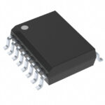 TP3054WM-X/63

The activity of extra discounts on wholesale prices is in full swing…
Please fill in your contact information and we will send you the latest wholesale price list.







