ChipApex | Global Electronic Components Supplier
SEARCH
Search Product
Search Post
— IC芯片 | 连接器 | 传感器 | 被动器件 —
Search productSearch post
— IC芯片 | 连接器 | 传感器 | 被动器件 —
Consult the customer manager about the wholesale price.
consultation hotline:86-132-6715-2157
email:[email protected]
Contact the product manager for consultation. One-stop consultation is available.
Do you want a lower wholesale price? Please send us your inquiry and we will reply immediately.
The TP5551-TR is a single-channel, chopper-stabilized zero-drift operational amplifier manufactured by 3PEAK. It operates on a supply voltage range of 1.8 V to 5.5 V and features ultra-low input offset voltage (max 5 μV) and minimal temperature drift (0.05 µV/°C max). The device provides a gain-bandwidth product of 3.5 MHz and a slew rate of 2.5 V/μs with rail-to-rail input and output capabilities. Quiescent current is typically 1400 μA per amplifier at 5 V. It includes high CMRR and PSRR (up to 130 dB), 7 kV HBM ESD protection, and operates within a temperature range of -40°C to 125°C.
Verify the specific package suffix matches the required footprint; TP5551-TR indicates SOT23-5 packaging. Confirm RoHS compliance and halogen-free status for environmental regulations. Ensure design accounts for the specified MSL level during PCB assembly processes. Validate that input currents remain within limits if signals exceed supply rails by more than 300 mV to prevent damage from forward-biased ESD diodes.
Select this component when ultra-low offset voltage and negligible drift are critical for DC precision applications. Consider the 1400 μA quiescent current consumption relative to system power budgets. Evaluate the need for external filtering to suppress residual ripple at the chopping frequency. Ensure source impedance balancing is implemented to minimize input offset current effects in high-impedance circuits.
This part belongs to the TP555X family of zero-drift amplifiers, which also includes dual (TP5552) and quad (TP5554) variants. The family shares core electrical characteristics such as bandwidth, noise profile, and supply voltage ranges. The TP5551 specifically denotes the single-amplifier configuration optimized for space-constrained designs using compact surface-mount packages like SOT23-5.
Direct functional substitutes within the same family include TP5552 and TP5554, though channel counts differ. Cross-manufacturer replacements require matching zero-drift topology, 3.5 MHz bandwidth, and 5 μV offset voltage specifications. Verify pinout compatibility and thermal resistance values if replacing in existing layouts.
The chopper stabilization reduces flicker noise significantly, eliminating the 1/f noise corner down to 0.1 Hz. This results in very low voltage noise density of 15 nV/√Hz at 1 kHz and 0.35 μVpp between 0.1 Hz and 10 Hz.
Charge injection from the chopper switches can cause apparent shifts in input bias current. To minimize total input offset current, the input impedance should be balanced across both IN+ and IN- terminals, and a guard ring layout is recommended to reduce PCB surface leakage.
While internal notch filters suppress most chopping-related ripple, residual noise exists at the chopping frequency and its harmonics. If the input signal frequency is near the chopping frequency, placing a post-filter at the output is recommended to further suppress interference.
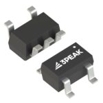 TP5551-TR
The activity of extra discounts on wholesale prices is in full swing…
Please fill in your contact information and we will send you the latest wholesale price list.