 ChipApex | Global Electronic Components Supplier
SEARCH
Search Product
Search Post
— IC芯片 | 连接器 | 传感器 | 被动器件 —
Search productSearch post
— IC芯片 | 连接器 | 传感器 | 被动器件 —
Consult the customer manager about the wholesale price.
consultation hotline:86-132-6715-2157
email:[email protected]
Contact the product manager for consultation. One-stop consultation is available.
Do you want a lower wholesale price? Please send us your inquiry and we will reply immediately.
The TPIC6A259DW is an 8-bit addressable latch with open-drain DMOS outputs, designed for general-purpose storage in digital systems. It operates within a logic supply voltage range of 4.5 V to 5.5 V and supports a power DMOS drain-to-source voltage up to 50 V. The device provides eight independent 350-mA outputs with short-circuit protection and features four distinct function modes: addressable latch, memory, demultiplexer, and clear. It includes separate power ground (PGND) and logic ground (LGND) terminals to minimize parasitic impedance and crosstalk. Characterized for operation over a case temperature range of -40°C to 125°C, it is available in a 24-pin wide-body surface-mount package.
Verify the specific ordering suffix against the Package Option Addendum to confirm the correct packaging type, such as tube or tape and reel. Ensure the component matches the required RoHS compliance status and lead finish specifications. Confirm that the selected variant aligns with the intended manufacturing process and moisture sensitivity level requirements for your assembly line.
Select this component when designing circuits requiring high-voltage switching capabilities combined with flexible data storage functionality. The separate ground terminals are critical for applications needing isolation between control logic and power loads. Consider the thermal resistance characteristics and derating factors when determining heat dissipation requirements for the chosen package style under maximum load conditions.
This part belongs to the TPIC6A259 family of power logic devices manufactured by Texas Instruments. It is characterized for industrial temperature ranges and offers both through-hole and surface-mount package options. The device integrates DMOS technology to provide high-current driving capabilities while maintaining low on-state resistance for efficient power management in various digital control applications.
TPIC6A259DWRG4
Each open-drain DMOS transistor features an independent chopping current-limiting circuit designed to prevent damage in the event of a short circuit.
Separate power ground (PGND) and logic ground (LGND) terminals are provided to facilitate maximum system flexibility and minimize parasitic impedance. A single-point connection should be made externally to reduce crosstalk between logic and load circuits.
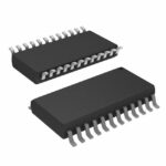 TPIC6A259DW
The activity of extra discounts on wholesale prices is in full swing…
Please fill in your contact information and we will send you the latest wholesale price list.





