 ChipApex | Global Electronic Components Supplier
SEARCH
Search Product
Search Post
— IC芯片 | 连接器 | 传感器 | 被动器件 —
Search productSearch post
— IC芯片 | 连接器 | 传感器 | 被动器件 —
Consult the customer manager about the wholesale price.
consultation hotline:86-132-6715-2157
email:[email protected]
Contact the product manager for consultation. One-stop consultation is available.
Do you want a lower wholesale price? Please send us your inquiry and we will reply immediately.
The TPW4066-TR is a quad single-pole single-throw (SPST) analog switch manufactured by 3PEAK, designed for analog and digital multiplexer or demultiplexer applications. It features four independent switches controlled by dedicated digital select inputs (S1–S4). The device supports supply voltages of 3.3 V, 5 V, and 10 V, with an operating range from 3 V to 12 V. Key electrical parameters include a typical bandwidth of 200 MHz at 5 V/10 V supplies and fast switching times of tON = 60 ns and tOFF = 50 ns. On-state resistance varies with voltage: typically 300 Ω at 3 V, 60 Ω at 4.5 V, and 50 Ω at 9 V. It operates within a temperature range of –40°C to 125°C and utilizes TSSOP14 packaging.
Verify the specific package variant when ordering, as the TPW4066-TR designation corresponds to the TSSOP14 package in the official order information. Confirm that the required quantity aligns with the standard tape and reel count of 3,000 units per manufacturer specification. Ensure design compatibility with the –40°C to 125°C operating temperature range and validate ESD protection requirements against the specified HBM and CDM levels before finalizing procurement.
Select the TPW4066-TR when a quad SPST configuration is required for signal routing in space-constrained designs utilizing TSSOP14 packages. Consider this component for applications demanding high bandwidth up to 200 MHz and low on-state resistance at higher supply voltages. Evaluate the trade-off between the 300 Ω resistance at 3 V operation versus lower resistance at 5 V or 10 V if signal integrity under varying load conditions is critical to the system performance.
The TPW4066 belongs to the 3PEAK analog switch family, which includes multiplexers like the TPW4051 and TPW4052. Unlike these multi-channel selectors, the TPW4066 provides four independent SPST channels, offering greater flexibility for parallel signal paths. It shares similar performance characteristics, such as 200 MHz bandwidth and 12 V maximum supply rating, with other devices in the series but distinguishes itself through its specific pinout and independent control architecture.
Public confirmed substitute part numbers are not available in the provided documentation.
The absolute maximum supply voltage (VCC to GND) is 13 V, with recommended operating conditions supporting up to 12 V.
The typical on-state resistance decreases as supply voltage increases: it is approximately 300 Ω at 3 V, 60 Ω at 4.5 V, and 50 Ω at 9 V.
Yes, the device input range extends to the supplies, allowing it to operate effectively with signals spanning the full supply voltage range.
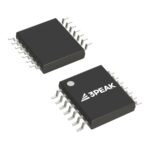 TPW4066-TR
The activity of extra discounts on wholesale prices is in full swing…
Please fill in your contact information and we will send you the latest wholesale price list.





