 ChipApex | Global Electronic Components Supplier
SEARCH
Search Product
Search Post
— IC芯片 | 连接器 | 传感器 | 被动器件 —
Search productSearch post
— IC芯片 | 连接器 | 传感器 | 被动器件 —
Consult the customer manager about the wholesale price.
consultation hotline:86-132-6715-2157
email:[email protected]
Contact the product manager for consultation. One-stop consultation is available.
Do you want a lower wholesale price? Please send us your inquiry and we will reply immediately.
The TS2012 is a fully differential, Class D stereo audio power amplifier designed for filter-free applications. It operates within a supply voltage range of 2.5 V to 5.5 V and delivers up to 2.8 W into a 4 Ω load at 5 V with 10% THD+N. The device features four selectable gain settings (6, 12, 18, or 24 dB) configured via G0 and G1 pins. It includes independent active-low standby control for each channel, pop-and-click reduction circuitry, and thermal shutdown protection. The component is housed in a lead-free QFN20 4x4 mm package.
Verify the specific ordering suffix against the manufacturer's official documentation to confirm exact packaging and tape/reel specifications. Ensure the procurement source provides valid traceability for this production data part number. Confirm that the received components match the QFN20 4x4 mm lead-free package requirements specified in the datasheet.
Select this component for portable audio designs requiring high efficiency without external LC filters. It is suitable for systems operating between 2.5 V and 5.5 V where low current consumption and minimal external component count are priorities. Verify that the application supports fully differential inputs or utilizes appropriate single-ended to differential conversion.
This component belongs to STMicroelectronics' portfolio of Class D audio power amplifiers. It is engineered to provide high efficiency compared to traditional Class AB amplifiers while maintaining compact form factors. The design targets consumer electronics where space constraints and battery life are critical considerations.
Consult the official datasheet revision history and cross-reference lists for confirmed substitute part numbers. Do not assume pin compatibility with other Class D amplifiers without verifying electrical characteristics and pinout configurations.
The gain is set using two discrete pins, G0 and G1. Logic levels on these pins select one of four gains: 6, 12, 18, or 24 dB.
The common-mode feedback loop controls the output bias value to average it at VCC/2, maximizing output voltage swing and allowing operation with any DC common-mode input voltage.
Input coupling capacitors are optional. The common-mode feedback loop allows the device to operate without them, though they can be added to define a low-frequency cutoff.
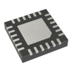 TS2012IQT
The activity of extra discounts on wholesale prices is in full swing…
Please fill in your contact information and we will send you the latest wholesale price list.






