 ChipApex | Global Electronic Components Supplier
SEARCH
Search Product
Search Post
— IC芯片 | 连接器 | 传感器 | 被动器件 —
Search productSearch post
— IC芯片 | 连接器 | 传感器 | 被动器件 —
Consult the customer manager about the wholesale price.
consultation hotline:86-132-6715-2157
email:[email protected]
Contact the product manager for consultation. One-stop consultation is available.
Do you want a lower wholesale price? Please send us your inquiry and we will reply immediately.
The TS3004ITD1033 is a single-supply oscillator and timer from Silicon Labs, operating within a voltage range of 1.55V to 5.25V. It consumes a maximum supply current of 2.4 µA at 25°C and 3.6 µA across the -40°C to +85°C temperature range. The device features a user-programmable output period adjustable from 3.3µs to 233s via an external resistor on the RSET pin and frequency divider inputs. It provides separate FOUT and PWMOUT signals with a 160Ω driver resistance. The component is housed in a 10-pin, 3x3mm TDFN package with an exposed paddle.
Verify that the ordering suffix 'T' indicates tape and reel packaging for quantities of 3000 units. Confirm lead-free compliance as standard for this product line. Ensure the application circuit accounts for the 10-pin TDFN thermal requirements and proper grounding of the exposed paddle for optimal performance.
Select the TS3004 when ultra-low power consumption is critical compared to traditional 555-timer solutions. Choose this model if the design requires a programmable period up to 233s without complex external components. Consider the 10-pin TDFN package constraints for PCB layout, specifically managing capacitive loads on FOUT and PWMOUT to minimize transient power consumption.
The TS3004ITD1033 belongs to Silicon Labs' CMOS timer family, which includes the TS3001, TS3002, TS3003, and TS3006. These devices are categorized under NanoWatt Analog high-performance analog integrated circuits. The ITD1033 variant specifically denotes the industrial temperature range (-40°C to +85°C) and the specific tape and reel packaging configuration.
Public datasheets do not list direct cross-references or substitute part numbers for the TS3004. Designers replacing legacy 555-timers should note the significant reduction in PCB area and power consumption but must redesign the timing network using the specified RSET resistor and FDIV inputs.
The FOUT period is determined by the formula tFOUT(s) = 8 * FDIV2:0 * RSET / 1.08E11, where FDIV2:0 represents the logic state of the frequency divider inputs and RSET is the resistance value connected to the RSET pin.
The PWMOUT signal is anti-phase with respect to the FOUT output. A dead time of approximately 106ns exists between the falling edge of FOUT and the rising edge of PWMOUT.
To disable the PWM function and reduce current consumption, connect the CPWM pin directly to VDD. This action saves the current typically drawn by the PWM circuitry.
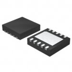 TS3004ITD1033
The activity of extra discounts on wholesale prices is in full swing…
Please fill in your contact information and we will send you the latest wholesale price list.




