 ChipApex | Global Electronic Components Supplier
SEARCH
Search Product
Search Post
— IC芯片 | 连接器 | 传感器 | 被动器件 —
Search productSearch post
— IC芯片 | 连接器 | 传感器 | 被动器件 —
Consult the customer manager about the wholesale price.
consultation hotline:86-132-6715-2157
email:[email protected]
Contact the product manager for consultation. One-stop consultation is available.
Do you want a lower wholesale price? Please send us your inquiry and we will reply immediately.
The TS5N412DBQR is a high-bandwidth FET bus switch manufactured by Texas Instruments, housed in a 16-pin SSOP (DBQ) package. It functions as a 4-bit 1-of-2 multiplexer/demultiplexer with a single output-enable input. The device utilizes a charge pump to elevate the gate voltage of pass transistors, ensuring low and flat ON-state resistance for minimal propagation delay and rail-to-rail switching on data I/O ports. It operates within a supply voltage range of 4.75 V to 5.25 V and supports bidirectional data flow between A and B ports when enabled. Key electrical parameters include a typical ON-state resistance of 3 Ω at 5 V, a maximum propagation delay of 3 ns, and an OFF isolation of -50 dB at 25 MHz.
Verify the ordering suffix DBQR corresponds to the tape and reel packaging format containing 2500 units per large reel. Confirm the top-side marking YB412 matches the specific production lot requirements. Ensure the component meets RoHS compliance standards and Level-2 moisture sensitivity ratings suitable for surface-mount assembly processes.
Select this component for high-bandwidth applications requiring optimized interfaces for broadband communications or networking. The device is suitable for data-intensive computing systems where low capacitive loading minimizes signal distortion. Consider the 4.75 V to 5.25 V operating range and the requirement for a pullup resistor on the OE pin to ensure high-impedance states during power transitions.
This part belongs to the TS5N412 series of 4-bit 1-of-2 FET multiplexers and demultiplexers. The DBQR suffix specifically denotes the shrink small-outline package variant supplied in tape and reel format. It shares functional specifications with the PW package version but differs in physical dimensions and manufacturing packaging logistics.
The TS5N412PW serves as a direct functional alternative utilizing a TSSOP package. Verify pinout compatibility and thermal impedance differences between the DBQ and PW packages before substitution.
The device features Ioff circuitry that prevents damaging current backflow through the switches when the device is powered down, ensuring isolation during power-off states.
The typical ON-state resistance is 3 Ω at a supply voltage of 5 V, providing low and flat resistance characteristics across the operating range.
The OE pin should be tied to VCC through a pullup resistor to ensure the high-impedance state exists during power transitions; the minimum resistor value depends on the driver's current-sinking capability.
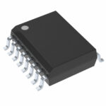 TS5N412DBQR
The activity of extra discounts on wholesale prices is in full swing…
Please fill in your contact information and we will send you the latest wholesale price list.





