 ChipApex | Global Electronic Components Supplier
SEARCH
Search Product
Search Post
— IC芯片 | 连接器 | 传感器 | 被动器件 —
Search productSearch post
— IC芯片 | 连接器 | 传感器 | 被动器件 —
Consult the customer manager about the wholesale price.
consultation hotline:86-132-6715-2157
email:[email protected]
Contact the product manager for consultation. One-stop consultation is available.
Do you want a lower wholesale price? Please send us your inquiry and we will reply immediately.
The TS5N412PW is a 4-bit 1-of-2 FET multiplexer/demultiplexer and high-bandwidth bus switch manufactured by Texas Instruments. It operates within a supply voltage range of 4.75 V to 5.25 V and supports data I/O voltages from 0 V to 10 V. The device features a propagation delay of 3 ns, an ON-state resistance (ron) typically ranging from 3 Ω to 12.5 Ω depending on conditions, and low input/output capacitance with a maximum of 20 pF for the B port in the OFF state. It utilizes a charge pump to elevate gate voltage, ensuring flat ON-state resistance characteristics over the operating range. The component is housed in a TSSOP-16 package and functions across an operating temperature range of -40°C to +85°C.
Verify the specific ordering suffix against the manufacturer's current documentation to confirm packaging type and moisture sensitivity level. Ensure the procurement matches the required tape and reel or tube configuration as specified in the latest package addendum. Confirm RoHS compliance status and lead finish details directly from the official datasheet before finalizing orders.
Select this component for high-bandwidth applications requiring precise signal routing between digital and analog domains. Consider the 4.75 V to 5.25 V supply requirement and the 0 V to 10 V I/O voltage range when designing the system interface. Evaluate the thermal impedance and package constraints to ensure adequate heat dissipation within the specified -40°C to +85°C operating temperature range.
The TS5N412 belongs to the TS5N412 series of logic ICs, specifically categorized under encoders, decoders, multiplexers, and demultiplexers. It is designed to support broadband communications, networking, and data-intensive computing systems. The device provides an optimized interface solution for high-speed data transfer environments where low distortion and high isolation are critical requirements.
The TS5N412DBQR is a functionally equivalent part number within the same family, differing primarily in its SSOP (DBQ) package and tape-and-reel shipping format instead of the TSSOP tube packaging.
The device is fully specified for partial-power-down applications using Ioff circuitry, which prevents damaging current backflow through the device when it is powered down, ensuring isolation during power off.
With a 50 Ω load and a 0.632 V P-P input signal, the TS5N412 achieves a bandwidth of 25 MHz, defined as the frequency at which the gain is -3 dB below the DC gain.
The device meets JESD 22 standards with a 2000-V Human-Body Model rating (A114-B, Class II) and a 1000-V Charged-Device Model rating (C101).
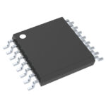 TS5N412PW
The activity of extra discounts on wholesale prices is in full swing…
Please fill in your contact information and we will send you the latest wholesale price list.





