 ChipApex | Global Electronic Components Supplier
SEARCH
Search Product
Search Post
— IC芯片 | 连接器 | 传感器 | 被动器件 —
Search productSearch post
— IC芯片 | 连接器 | 传感器 | 被动器件 —
Consult the customer manager about the wholesale price.
consultation hotline:86-132-6715-2157
email:[email protected]
Contact the product manager for consultation. One-stop consultation is available.
Do you want a lower wholesale price? Please send us your inquiry and we will reply immediately.
The UCC23513QDWYRQ1 is an automotive-grade, single-channel opto-compatible reinforced isolated gate driver designed for IGBT, MOSFET, and SiC MOSFET applications. It features a peak source current of 4.5A and a peak sink current of 5.3A. The device provides a reinforced isolation rating of 5.7kVrms with a minimum common-mode transient immunity (CMTI) of 150kV/μs. It operates within a supply voltage range of 14V to 33V and supports junction temperatures from -40°C to +150°C. Key timing parameters include a maximum propagation delay of 105ns, inter-device delay matching of 25ns, and pulse width distortion of 35ns.
Verify the Q1 suffix confirms AEC-Q100 automotive qualification status before integration into safety-critical designs. Confirm the DWYR package variant matches PCB footprint requirements. Ensure ESD protection measures are implemented during handling due to humidity sensitivity classification. Validate that the specific revision level meets project documentation standards.
Select this component when replacing standard optocouplers to achieve higher CMTI and longer isolation life without layout changes. Suitable for high-side and low-side driving configurations requiring wide supply voltage ranges up to 33V. Ideal for SiC and IGBT applications demanding precise timing synchronization and high thermal stability.
This part belongs to the UCC23513 family of isolated gate drivers. It serves as a direct pin-to-pin upgrade for legacy opto-isolated gate drivers, maintaining schematic compatibility while significantly improving electrical performance metrics such as delay matching and transient immunity.
Direct replacement for UCC23513DWR. Verify UCC23513BQDWYRQ1 for identical automotive specifications if sourcing alternatives.
The device specifies a minimum CMTI of 150kV/μs.
Yes, the input stage can handle up to 13V of reverse polarity voltage.
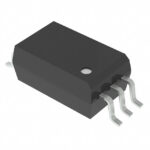 UCC23513QDWYRQ1
The activity of extra discounts on wholesale prices is in full swing…
Please fill in your contact information and we will send you the latest wholesale price list.





