 ChipApex | Global Electronic Components Supplier
SEARCH
Search Product
Search Post
— IC芯片 | 连接器 | 传感器 | 被动器件 —
Search productSearch post
— IC芯片 | 连接器 | 传感器 | 被动器件 —
Consult the customer manager about the wholesale price.
consultation hotline:86-132-6715-2157
email:[email protected]
Contact the product manager for consultation. One-stop consultation is available.
Do you want a lower wholesale price? Please send us your inquiry and we will reply immediately.
The UCC2837D is an 8-pin N-FET linear regulator controller manufactured by Texas Instruments. It operates from input voltages as low as 3V and supports output voltages down to 1.5V. The device features a built-in charge pump for external N-MOSFET gate drive, duty ratio mode overcurrent protection, and extremely low dropout voltage characteristics. Electrical specifications include a supply current of 1.5mA at VDD=5V, a reference voltage of 1.5V, and a comparator offset of 100mV. It functions within a temperature range of -25°C to +85°C and is housed in an SOIC-8 package.
Verify the specific ordering suffix (e.g., D) against the official TI datasheet to confirm the package type and operating temperature range. Ensure the selected variant matches the required industrial or commercial grade specifications. Cross-reference the manufacturer part number with authorized distributors to validate authenticity and traceability before finalizing procurement orders.
Select this component when designing linear regulators requiring extremely low dropout voltages and high efficiency using external N-MOSFET pass elements. Consider the internal charge pump limitations and ensure adequate capacitance on the CAP pin for stable gate drive. Evaluate the duty cycle timer capacitor requirements to properly configure overcurrent protection thresholds for the specific load conditions.
The UCC2837D belongs to the UCC3837 family of linear regulator controllers, which also includes the UCC1837 and UCC3837 variants differentiated primarily by their operating temperature ranges. This series is designed to replace standard three-terminal regulators where lower dropout and higher current capabilities are required. It utilizes a transconductance error amplifier and current sense amplifier for precise loop control.
Direct replacements within the same family include the UCC1837 and UCC3837, provided the extended or commercial temperature ranges align with system requirements. Verify pin compatibility and electrical parameters such as reference voltage and current limits when substituting.
It uses a duty ratio mode overcurrent protection technique. If the voltage across the current sense resistor exceeds the threshold, the device modulates the output driver at a specific duty cycle to limit average power dissipation during faults.
The CAP pin is the output of the internal charge pump circuit. It provides a floating bias voltage to drive the gate of the external N-channel MOSFET pass transistor. A minimum 0.01 µF ceramic capacitor is recommended between this pin and ground.
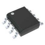 UCC2837D
The activity of extra discounts on wholesale prices is in full swing…
Please fill in your contact information and we will send you the latest wholesale price list.





