 ChipApex | Global Electronic Components Supplier
SEARCH
Search Product
Search Post
— IC芯片 | 连接器 | 传感器 | 被动器件 —
Search productSearch post
— IC芯片 | 连接器 | 传感器 | 被动器件 —
Consult the customer manager about the wholesale price.
consultation hotline:86-132-6715-2157
email:[email protected]
Contact the product manager for consultation. One-stop consultation is available.
Do you want a lower wholesale price? Please send us your inquiry and we will reply immediately.
The UCC5630AMWPTRG4 is a multimode SCSI terminator designed for SPI-2, SPI-3, and SPI-4 bus architectures. It automatically senses the bus via the DIFFB pin to switch between single-ended (SE) and low voltage differential (LVD) termination modes. The device operates on a TRMPWR supply ranging from 2.7V to 5.25V. In LVD mode, the REG output provides a typical voltage of 1.25V with a short-circuit source current of -420mA and sink current of 180mA. Differential impedance is typically 105 ohms with a bias voltage of 125mV. SE mode features an impedance of 110 ohms and termination currents between -18mA and -25.4mA depending on signal level. The component is housed in a 36-pin SSOP package.
Verify that the ordering suffix matches the required package type and environmental compliance. The 'MWP' designation indicates a 36-pin SSOP package, while 'TRG4' specifies tape and reel packaging with lead-free and halogen-free materials. Confirm the temperature range requirement aligns with the commercial grade specification of 0°C to 70°C before finalizing procurement orders.
Select this component when designing SCSI terminators that must support mixed legacy single-ended and modern low voltage differential devices without manual configuration. Ensure the design accommodates the specific capacitance balance requirements of SPI standards. Verify that the power supply voltage remains within the 2.7V to 5.25V range to maintain proper regulator operation and termination accuracy.
This part belongs to the UCC5630A family of multimode SCSI terminators manufactured by Texas Instruments. It serves as a critical interface component for maintaining signal integrity in high-speed parallel SCSI environments. The device integrates multiple termination networks into a single monolithic solution, simplifying board layout compared to discrete implementations.
The UCC5630AFQP is a compatible alternative offering the same functionality in a 48-pin LQFP package. When substituting, verify pinout compatibility or implement necessary adapter circuitry due to the different physical footprint and pin assignments between the SSOP and LQFP packages.
The device monitors the DIFSENS line voltage through the DIFFB input pin. If the voltage is below 0.5V, it selects single-ended mode. Between 0.7V and 1.9V, it switches to low voltage differential mode. Above 2.4V, it enters a high impedance state to disconnect from high voltage differential buses.
The MSTR/SLV pin controls the DIFSENS driver. When connected to TRMPWR, it enables the driver, allowing the device to act as a master. When grounded, it disables the driver, configuring the device as a slave. This allows multiple terminators to share the bus while only one drives the sense line.
The HS/GND pins serve as heat sink grounds directly connected to the die mount paddle. They conduct heat away from the die to reduce junction temperature, which is essential for managing power dissipation, particularly in single-ended mode where instantaneous power per line can be significant.
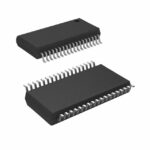 UCC5630AMWPTRG4
The activity of extra discounts on wholesale prices is in full swing…
Please fill in your contact information and we will send you the latest wholesale price list.





